Making Her Mark: Q&A with Professor Michal Lipson
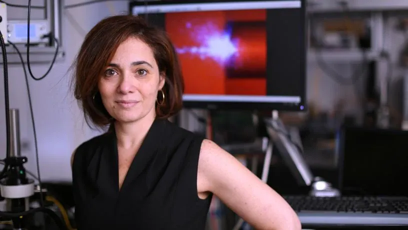
Michal Lipson is a pioneer whose seminal research underpins the explosive growth and rapid commercialization of silicon photonics, a technology that uses optical rays to transfer data among computer chips. In 2015, she joined Columbia Engineering—as the Eugene Higgins Professor of Electrical Engineering and professor of applied physics—where she heads the Lipson Nanophotonics Group. Lipson’s trailblazing work has been recognized numerous times by her peers. A 2010 MacArthur Foundation Fellow, winner of the 2019 Comstock Prize in Physics from the National Academy of Sciences, and recipient of the 2019 IEEE Photonics Award and the 2017 OSA R. W. Wood Prize, she is also one of the most highly cited researchers in modern physics, as coauthor of more than 200 scientific publications. In December 2018, she was awarded an honorary doctorate by Trinity College at the University of Dublin. She currently holds more than 30 US patents and has founded two startups based on these technologies—one of them using Lidar for autonomous vehicles. She spoke with Columbia Engineering about the joy of physics, putting all your eggs in one basket, and young female researchers taking charge of their careers.
You received your BS, MS, and PhD—all in physics—from Technion Israel Institute of Technology. How did you get interested in physics?
I grew up in a family of physicists. My father is a cosmologist and my mother also did research in physics. My father loved—still loves— what he does so much that it was almost a question of “Why wouldn’t you do it?” This is a job where you get paid to think about new ideas, to collaborate with young people, to create, to revolutionize technology or science. It’s an incredible job.
So you followed your father’s path into physics?
I have a twin sister, Merav Opher, and she’s is a professor in space physics at Boston University. Both of us were born in Israel, although my father and mother were born in the Bronx. My father is a Harvard graduate who did his PhD with Nobel Prize winner Norman Ramsey (BS’35), in an area that is actually close to mine. My parents emigrated in their late 20s to Israel, where my sister and I were born. When we were eight years old, we moved to Brazil so that my father could pursue his work in astrophysics and work with radio telescopes in São Paulo. When I was nineteen I went back to Israel to finish my undergrad in physics, and then I pursued a PhD in solid state physics at the Technion, where my father had been a professor.
You went to MIT as a postdoc in material sciences. How did you end up branching out?
When I started, my PhD work was in fundamental semiconductor physics. I studied the physics of semiconductor optical cavities. At MIT, I joined Professor Lionel Kimerling’s group, who focused on material science aspects and applications of semiconductor cavities. I liked these aspects a lot, and I started transitioning from basic physics toward more applied physics and devices. At Cornell, I joined the electrical engineering department, which was more about developing devices based on the materials and physics that I had learned.
Did that move to electrical engineering and more applied work evolve, or was it planned?
I just gave a plenary talk at the National Conference for Women Undergrads in Physics about how I picked the subject of silicon photonics. I think this was a very good decision. It had three aspects that I think are really important, especially for a woman. The first one was to choose a research area that would be objective and would have clear metrics of success. I was looking for an area with clear goals, where whoever gets the objective—which ideally would be an actual number (such as efficiency, speed, etc.)—would be the winner. For a woman, it’s very important to pick a subject with concrete metrics because it’s politics-free. I was also looking for a topic where I would be independent. At the time, traditional semiconductor materials were a little problematic because there were only a few people who grew these samples, so if you wanted to work in this area you basically depended on others. As a young female, I didn’t have those connections, and even if I did, I didn’t want to put my career in the hands of someone else. I picked silicon photonics because silicon devices could be fabricated anywhere and I could do it completely by myself. The last aspect of my decision to invest in silicon photonics was the prospect of the area to have a very large impact on technology. The requirements and challenges in this area were very hard—one would actually have to realize photonics with a material that was not an optical material at all; it was only used for electronics at the time. But I felt that if one could do it, it would completely revolutionize technology. So it was a really good topic.
A major thrust of Lipson's work focuses on externally controlling the optical properties of silicon.
When you entered the field, silicon photonics was something no one had really thought to explore.
In 2001, at the beginning of my career, working in silicon photonics was very unconventional. Almost no one was working on this topic. In my talks, I used to see a lot of people in the audience rolling their eyes. After I published a paper in Nature in 2004 showing that one could actually electrically change the optical properties of silicon by applying voltage, there was a real turning point in the field. It was the first time that one could externally control the optical properties of silicon devices and route light on demand. It was a big deal because to enable optical circuits on silicon, you have to be able to manipulate the material externally. So for me to have published this paper with no connections—I wasn’t known, I was a nobody—was a very big deal.
Despite that, in my threeyear review, the feedback from the department was that I was putting all my eggs in one basket and I should move to a different topic; that silicon photonics was too risky. But only a year later, I published another Nature paper actually showing electrical modulation of light traveling in silicon. After that, everything exploded.
That was in 2005?
Yes, by 2005, silicon photonics became the hottest thing. Everyone that used to do semiconductor physics transitioned to silicon photonics. People who used to do optics in semiconductors and other traditional optical material all transitioned because objectively silicon photonics made sense. But objectively, when one looked at the numbers, even back in 2001, it made sense. I just had to actually experimentally demonstrate that it is possible.
What were you able to see in the numbers?
Transmitting information over light is fundamentally low power even when one transmits very high bandwidths. You can transmit a lot of information with basically no power dissipation and no heat. That’s a must for any application where a lot of data needs to be transmitted—optical communications, data communication. And silicon is transparent at near-infrared light.
But why is it so cheap to implement?
The Si [silicon] microelectronics processing is very developed. There is a billion-dollar infrastructure already in place enabling this technology. People had developed the “recipes” for making structures with incredible quality, with atomic precision; and we took those recipes and the machines and started making optical devices. It turns out that these silicon optical devices were much, much better than those made from other traditional materials, because the infrastructure was in place; the material, all the recipes, everything was there already.
Is that when you won the MacArthur Fellowship, commonly known as the “genius grant”?
Exactly. That was in 2010, and the field was exploding. It is still exploding. We are now working with major companies building computing systems and data centers. So now it’s actually real. Silicon photonics is so mature that there are many, many other applications—anything related to optics. Today almost any optical system—for medical diagnostics, microscopy, autonomous vehicles, Lidar—you could realize with silicon photonics.
What did the MacArthur mean for your research? What did it mean for you personally?
By that time, I knew that the research was a success. But it was very important for me as a person to have the recognition. Science is all peer reviewed, so those recognitions are very important because they propel us forward, they give us a motivation.
Where might your research take you next?
Now we are looking at many different applications. Since coming to Columbia we already founded two—we founded one company to make Lidar for autonomous vehicles.
What drew you to Columbia from Cornell?
I loved Cornell. There is something about being more isolated that increases your career activity and creativity. It’s the same reason why young PhD students sometimes get crazy ideas; they are not yet “polluted” and perhaps not as skeptical. But I felt that it was time for me to refresh the topics that I was working on, and there were many colleagues that I was looking to interact with—specifically, Keren Bergman, who is one of my strongest collaborators. For me to be near her was fantastic. And there were many other people here that I felt would be a really good addition to my work.
Drawing lessons from your own life, what advice would you give parents who want to foster a love of science and engineering in their children?
When I was growing up, my father always told my sister and me to “make a mark.” You might think that saying to a 12-year-old “make a mark” would put incredible pressure on her, but what it meant for me is that he really believed I could make a mark. For him there was no question whether we could do it or not. And that meant the world, the fact that he believed that both my sister and I could completely revolutionize whatever field we chose.
He also directed us very specifically. I think today there is a sense that youngsters should be left to choose what they want to pursue, but that assumes that the affinity to an area is an inherent quality, that it cannot be acquired. My father was not in that school. He felt that physics is a very broad area, and that there are many ways to do research—that we would shape our research and our work environment and make it our own. And that is exactly what happened. I feel that my research group reflects who I am. I have 20 students that constantly brainstorm together. It’s a very social environment. And my father works part-time in my group. And he often asks them the same questions that I ask: “Why is this important?” He ensures that the big picture is always there.
What do you do in your spare time?
I have two boys, Lahav who is 22 and Ethan who is 14, and I cherish my time with them. Lahav is a senior at Columbia in computer science. He is on track to graduate summa cum laude this spring and now plans to pursue his PhD in computer science. Ethan is at Stuyvesant, where my father went to high school, and is already hooked on computer science as well.
What qualities do you try to instill in your boys?
I feel very strongly that if there’s one—or maybe two— qualities that one should instill in the kids it should be confidence and grit, or resilience.
PORTRAIT PHOTO CREDIT: JOHN ABBOTT | LAB PHOTO CREDIT: TIMOTHY LEE PHOTOGRAPHERS
ORIGINAL ARTICLE HERE.