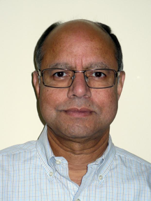
Biography:
Kadaba R. (Kumar) Lakshmikumar received his B.E. and M.E. degrees in Electrical Communication Engineering from the Indian Institute of Science, Bangalore, India, and Ph.D. degree in Electrical Engineering from Carleton University, Ottawa, Canada. He did pioneering work in the area of modeling mismatch in MOS devices for his doctoral work. The standard deviation of mismatch was shown to be inversely proportional to the square-root of the channel area. His paper in the December 1986 issue of the IEEE Journal of Solid-State Circuits is among the top 20 cited publications of the journal between 1968 and 1992.(http://www.ieee.org/organizations/pubs/newsletters/sscs/oct02/TopArticles.html.)
Lakshmikumar has made lasting contributions to the field of IC design through his leadership in identifying and solving technically challenging problems. He presented a tutorial titled “PLL Design in Nanometer CMOS” at ISSCC 2010. The tutorial (http://sscs.ieee.org/tutorials-on-line/2010-issccshort-courses-and-tutorials/426-isscc-2010-tutorial-pll-design-in-nanometer-cmos.html) illustrates design techniques for overcoming large variability, low supply voltage and high leakage. In 2015, he presented a short course, “Clock and Data Recovery Techniques for Optical Communication Systems” at CSICS.
