In direct comparison, an asynchronous network-on-chip design outperforms a commercial synchronous chip
Working with colleagues in academia and industry, Steven Nowick and his group have conducted the first direct experimental comparison between an asynchronous network-on-chip (NoC) design and a leading industrial synchronous NoC chip implemented in advanced technology (14 nm FinFET). The synchronous chip was manufactured by Advanced Micro Devices (AMD) and is currently used in several commercial products. Results from the experiments, which were carried out on a single network node on the asynchronous NoC design, show the NoC design performed significantly better when compared to a synchronous chip—55% less area with 28% lower latency—along with a 58% reduction in active power and an 88% reduction in idle power.

While these results were mostly in line with our expectations, they are exciting as validation of our research. In particular, a major achievement was attaining significantly smaller circuit area,” says Nowick, who with his PhD student Weiwei Jiang designed the asynchronous on-chip network along with colleagues at the University of Ferrara in Italy (Professor Davide Bertozzi, PhD student Gabriele Miorandi). “People think of asynchronous chips as often being larger than their synchronous counterparts, but these results show that asynchronous designs can be much smaller than state-of-the-art NoCs in commercial products today. And they can be both faster and more energy-efficient.”

The experiments themselves were conducted at AMD in collaboration with AMD Fellows Greg Sadowski and Wayne Burleson. “This was a highly-productive and effective collaboration between Steve Nowick’s group and AMD,” says Sadowski. “His group’s asynchronous network-on-chip has great potential for our future systems, once the automated tool flow is developed.”
, the asynchronous design took up 55% less area, achieved 28% lower latency, and had an 88% savings in idle power and 58% savings in active power.")
A member of Columbia’s Data Science Institute (DSI), Nowick is the founder and chair of the new working group, Frontiers in Computing Systems, which has over 35 faculty members working at the intersection of computing systems, massive-scale application areas (science/medicine/engineering), and data science. The group is in the process of approval as new DSI center, to be called “Computing Systems for Data-Driven Science.”
The collaboration with AMD is part of Nowick’s long-term research into asynchronous digital design, which contrasts to the almost universally used synchronous systems, where operations and the flow of data are all synchronized to a fixed-rate global clock. Synchronizing operations ensures things happen in an orderly fashion but because all operations—fast or slow—begin and end according to the clock’s timing signals, there is built-in inefficiency since faster operations must wait on slower ones to complete. In addition, the central organizing clock is a poor match for heterogeneous distributed systems and scalability requirements: synchronizing the hundreds and even thousands of processor and memory components on some chips today is simply unmanageable at low cost using a monolithic synchronous paradigm.
Asynchronous systems, in contrast, have no clock, allowing components to operate independently of one another and at their own optimal speed, thus reducing the latencies that occur when idle components must wait for the next clock cycle to perform an operation. Dispensing with the clock is also more energy efficient. Asynchronous components are idle until needed, i.e., naturally operate “on demand.” The clock itself can consume 20-30% of the power on a chip. Aggressive synchronous techniques for turning off idle units—called “clock-gating”—are only partly effective, and have their own not-insignificant overheads. In addition, the asynchronous design style allows simpler and more streamlined design of storage components (i.e., registers and circular buffers) and pipeline control structures.
The question of course is, how does an asynchronous design compare to actual commodity asynchronous chips being manufactured today? To provide an answer, Jiang carried out the synchronous-asynchronous evaluation at AMD using standard industry simulation in varied traffic using a pre-layout asynchronous design originally developed at Columbia by Nowick working with Davide Bertozzi’s group at the University of Ferrara. (A detailed physical layout was eventually created from the design as proof of concept and to validate correctness, but was not used in the evaluation.) The original asynchronous NoC design was modified by Jiang during his six-month internship at AMD in Boxborough, Massachusetts, with the addition of his own new techniques for efficient virtual channels (VCs) to mitigate congestion.
To help quantify how much better an asynchronous design could do against the best industry chips, the two designs—one synchronous and the other asynchronous—were as similar in architecture as possible.
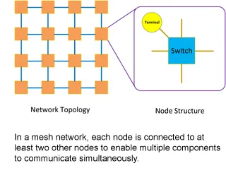
Both incorporate state-of-the-art NoC designs where components—processors, accelerators, memories—communicate over a network rather than over a simple shared bus or other simple channel that is controlled by a single master component at any time. To enable increasing numbers of components to operate in parallel—a growing necessity as chips began to incorporate hundreds or thousands of components—chip designers have looked to the networking community for ideas; the resulting “on-chip networks” ensure better congestion management, higher performance, and improved utilization of shared channel resources when compared to previous bus-based approaches.
Both designs are also energy-efficient: the asynchronous NoC design because its components, when not busy, are always in idle mode; and the synchronous NoC through fine-grained clock-gating.
What’s different, and what accounts for the better performance and energy efficiency, is the use of asynchronous communication in Nowick’s NoC as well as highly efficient asynchronous designs that largely use standard synchronous components. Details of this first direct comparison between an asynchronous design with actual leading-edge commodity hardware, supported by National Science Foundation funding, are described in the paper. An asynchronous NoC router in a 14nm FinFET library: Comparison to an industrial synchronous counterpart presented in March 2017 at the ACM/IEEE Design, Automation and Test in Europe (DATE) Conference, one of the top two international design conferences.

For its better performance and energy efficiency, as well as scalability and ease of assembly, asynchronous NoCs have been attracting attention for the past 10 years. Intel, IBM, STMicroelectronics, and other companies have all explored and published on their development of asynchronous chips. Especially ambitious is IBM’s 4,096-core, 5-billion-transistor “TrueNorth” chip (cover story, Science magazine [August 2014]), a neuromorphic design modeled on the brain, where the goal is to recreate millions of brain neurons and synapses in silicon, something clearly not possible to do efficiently using a synchronous communication network where everything is timed to a clock cycle.
Where TrueNorth is optimized for pattern recognition, Nowick and his students are designing general-purpose multicore NoCs with an eye to ease of manufacturing and time to market, as well as extremely low energy and high performance—all concerns that weigh heavily on an industry that has invested billions of dollars in synchronous designs and workflows. With a paradigm shift to asynchronous promising to be costly, Nowick and his students are pursuing a mixed synchronous/asynchronous approach called globally asynchronous, locally synchronous systems, or GALS, where components are synchronous, enabling the use of standard off-the-shelf commodity hardware, but the communication fabric is an asynchronous network able to accommodate varying operating speeds of chip components.
“The goal is to accommodate current architectural requirements and the use of existing synchronous components—processors, caches, accelerators—but entirely replace the synchronous communication structure with a “drop-in” asynchronous one,” says Nowick.
Still, new automated computer-aided design (CAD) tools will be needed before the industry can shift away from synchronous systems. To this end, Nowick is collaborating closely with University of Ferrara colleagues (Davide Bertozzi’s group) to modify commercial synchronous CAD tools to work effectively for asynchronous designs, and to develop a portable and high-quality automated design flow. (More information on developing an automated tool flow for designing and optimizing asynchronous NoCs can be found in their paper Accurate Assessment of Bundled-Data Asynchronous NoCs Enabled by a Predictable and Efficient Hierarchical Synthesis Flow, which appeared recently at the 2017 IEEE “Async” Symposium.)
After over 25 years researching asynchronous chip design, Nowick is seeing increasing interest with a flurry of projects starting up, especially as asynchronous design shows itself to be flexible in different contexts and applications, including neural networks. Nowick’s PhD student Kshitij Bhardwaj recently interned at Intel Labs, collaborating with researchers there to design an asynchronous NoC to support the multicast communication requirements of spiking neural networks.
In a new research project, Bhardwaj and Nowick, working with Prof. Luca Carloni and associate research scientist Paolo Montavani, will implement an asynchronous NoC in a GALS form in field-programmable gate arrays (FPGAs) for a large-scale accelerator-based multicore system, and apply it for both convolutional neural network (CNN) and wide area motion imagery (WAMI) applications (such as long-term monitoring of images for security and surveillance).
Other promising directions for asynchronous design include its use with emerging technologies, such as flexible electronics and carbon nanotubes, as well as in energy harvesting circuits, where large timing deviations and tight power constraints are extremely difficult to satisfy using fixed-rate clocking. Likewise, asynchronous designs have been explored to handle extreme environments (e.g., space missions) where circuits must be robust and operate correctly over a 400° C temperature range.
“I am very encouraged by our successful collaboration with AMD and the University of Ferrara in finally demonstrating the potential of asynchronous networks-on-chip for advanced commercial computing system” says Nowick. “In the next year or two, we hope to develop more complete and automated design tool flows, as well enable exciting new opportunities for FPGA-based parallel computing systems for energy-efficient neural network and vision applications.”
Original article can be found here.