Columbia, CUNY and Washington University team demonstrate the first topological insulator on a chip

Materials are typically classified into three categories – conductors, which can carry electricity, insulators, which do not, and semiconductors, which lie in between. Topological insulators, on the other hand, are an exotic state of matter which behave like conductors on the surface, but act as insulators underneath the surface. What is unique about topological insulators is that they achieve this behavior because of the topology of the band structures that define their conduction properties. Also unique is the fact that this behavior is symmetry-protected, meaning small imperfections or deformities cannot alter the surface propagation. The study of topological insulators has been an extremely active field of research in condensed matter physics recently, with the 2016 Nobel Prize awarded for the use of topological concepts in theoretical condensed matter physics.
The discovery and study of such electronic topological insulators (TIs) has also spurred the investigation of the equivalent of TIs in other domains, such as electromagnetic or photonic TIs, where electromagnetic (EM) waves can only travel on the surface, and cannot penetrate below. Today, in a paper reported in Nature Electronics researchers from Columbia University (Prof. Harish Krishnaswamy’s group or CoSMIC lab), City University of New York’s Advanced Science Research Center or ASRC (Prof. Andrea Alù’s group) and Washington University (Prof. Aravind Nagulu’s group) have demonstrated the first electromagnetic topological insulator on a chip, which derives its exotic features from suitably tailored patterns of temporal modulation.
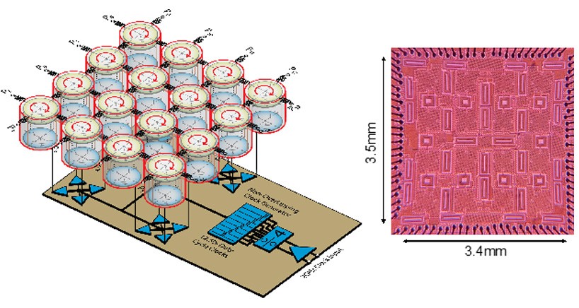
Profs. Alù, Krishnaswamy and Nagulu have been extremely active in the research of time-modulated materials, circuits and systems, where material or circuit parameters are varied periodically in time to overcome fundamental limits associated with traditional materials and circuits. One example of a fundamental limit that can be overcome is reciprocity, where a time-modulated system can have a wave propagate in different ways in forward and reverse directions. This can be used to realize non-reciprocal components, such as circulators and isolators, which find widespread use in various communication and radar systems. Building on this work, the team built an array or lattice of circulators to mimic the lattice structure of electronic topological insulators and realize the first TI for EM waves on a chip.

“Our demonstration represents an exciting discovery in the field of photonic topological insulators: our demonstration extends by orders of magnitude the bandwidth of operation and at the same time significantly scales down the footprint of our device, paving the way to extremely compact, broadband, highly reconfigurable nonreciprocal components based on topological matter,” said Prof. Alù.
Building such a TI for EM waves on a chip can bring this exotic physics into real world applications. Their chip can not only support the propagation of the EM wave on an edge or surface, but can also re-route the EM wave on demand by reconfiguring the individual circulators in the lattice, thus creating a fabric that flexibly and arbitrarily route EM waves. The team demonstrated how such a chip can be used for 5G wireless applications such as full-duplex multi-antenna wireless communications and multi-antenna impulse radar.
“This is an exciting collaboration between the fields of theoretical physics, applied electromagnetics and radio-frequency integrated-circuit design, and showcases how both new phenomena and new applications can be enabled by such a cross-disciplinary collaboration,” said Prof. Krishnaswamy.
This work was supported by the DARPA SPAR program, the AFOSR MURI program, the Office of Naval Research and the Department of Defense.