
Architecture
Simpified Architecture
We had many iterations of architecture before we were satisfied with all blocks. The final tape-outed version is V7.1. The top level block diagram is shown in Figure 1 and the expanded block diagram of NPU Core is shown in Figure 2. For the purpose of this website tab, these two simplified diagrams are enough for us to introduce each functional block. We also included the detailed verison of our architecture diagrams at the end of this tab, in case someone wants to dig deeper. For detailed description of each block and timing mechanism, please refer to the user manual that has been attached at the end of this tab.
Figure 1. Top level block diagram
Figure 2. NPU Core block diagram
There are three modules in the top level diagram in Figure 1, FSM, NPU Core and Registers. NPU Core is the core computing core that we designed for NN inference, its expanded version is shown in Figure 2. FSM stands for finite state machine, which is a controlling system that we designed to provide correct controlling signals to NPU Core based on the timing requirement. Registers, as the name entails, are a bunch registers that store configuration options of NPU Core. We call these registers SSFR (Stationary Special Function Registers), since they would remain stationary during one inference frame.
If we jump into NPU Core, there are many blocks working collaboratively to complete the entire inference. These blocks are introduced as follows:
MAC: MAC stands for Multiply and Accumulate and it is the core computation block for matrix multiplication. It is consisting of a multiplier, an adder, and a flop. For each block cycle it will take two new inputs, multiply them together, then add to the previously accumulated results.
ReLU: ReLU stands for Rectified Linear Unit. It is the hardware realization of the standard ReLU function, which finds the maximum value between the block input and zero. If the input is greater than zero, it will pass the input, whereras if the input is smaller than zero, it will output a zero.
PISO: PISO stands for Parallel-Input-Serial-Output. It will compress several parallel inputs and shift them out one by one. We used this block to reduce the number of output ports.
FIFO: FIFO stands for First-in-First-Out. It acts as a temporary results pool for NPU core so that user can choose to read the results later. This is a standard synchronous FIFO design, indicating there is only one clock for both reading and writing.
COMP: COMP stands for comparator. It takes two signed inputs and compares the larger one with the previous largest number encountered. If the larger one is greater than the previous largest, it will store the new largest value and record its index. We used this block to further accelerate the inference process of final NN layer.
MUX: MUX stands for multiplexer. It allows user to map the results of different blocks to output.
Debug: Debug stands for debugging engine. It has many probes on different blocks in the system and it can use these probes to take samples of signals and shift samples out one by one. We designed this engine for post-silicon debugging so that we can read chip internal signals.
Complete Architecture
There is a complex timing mechanism behind this architecture and everything has been documented in the user manual attached at the end of this tab. The followings are the complete top level block diagram and NPU Core diagram. These are good references when going through the timing diagram in Figure 5.
Figure 3. Complete top level block diagram
Figure 4. Complete NPU Core block diagram
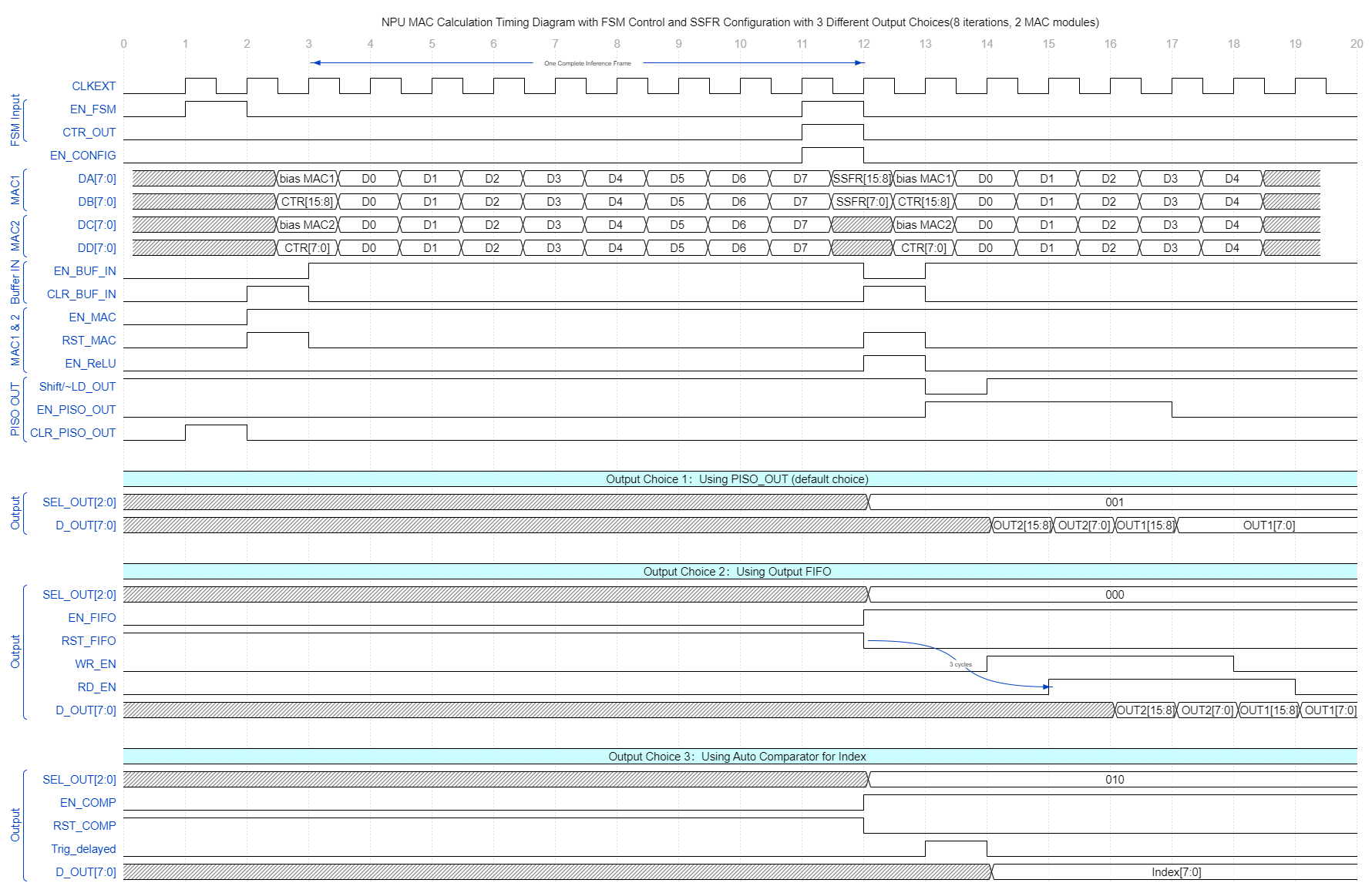
Figure 5. Timing diagram for different NPU operation modes