

Demo 1: RPI+NPU
Demo 1 Block Diagram & Setup
Our Demo 1 is a fairly complex demo, involving lots of programming and signal processing. The main purpose of this demo is to achieve a real-time interaction with audience during the demo session, so that audience can actually write a number by themselves and get it recognized. We used Raspberry Pi CM3 + IO expansion board (RPI) as the host controller for NPU. The entire system can be represented by the block diagram in Figure 1.
Figure 1. Demo 1 system-level block diagram
where RPI is connected to NPU PCB board using its header pins. These header pins were configured as standard GPIOs. A PC camera is connected to RPI so that it can capture a raw image for processing. Our laptop is connected to RPI wirelessly using ssh for monitoring the results. The complete setup of this demo is shown in Figure 2. The entire RPI+NPU system is sitting in the blue case, and there is a camera on top of the case, pointing to the white board in front of it. The adjacent laptop was showing the processing results. For first-order understanding, we annotated the recognition result back to the raw image on PC screen and it was showing "You've written the number 3", which agrees with the number on whiteboard.
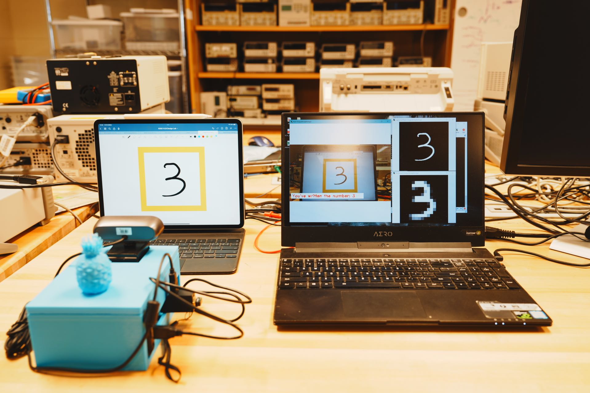
Figure 2. Demo 1 set-up
Demo 1 Preparation Methodology
We had a systematic approach to bring-up the chip for this demo and it turned out to be very effective, so we'd like to share this methodology in this section. The first thing we did was to make sure the host platform can provide the accurate timing we required, at least at a low frequency. Since RPI is not designed for strict timing control and we were just using pins as GPIOs, this is quite a challenging task. We had to establish a reliable timing control in a software environment, in this case C program, by utilizing serial executions of program on CPU. To realize this, we invented a timestamp mechanism as shown in Figure 3.
Figure 3. Timestamp mechanism in RPI to ensure timing match
We initiated a dedicated thread inside RPI for generating an accurate clock signal without the interference of other tasks. The clock was generated using naive delay() function and flipping IO voltage level. A counter will increment every time the clock signal is flipped, and it was used as a global reference clock edge for all the other functions. In software, we have two ways to achieve accurate timing control for each cycle, either we use an absolute method to specify the level of each signal at each cycle, or we use a relative approach to specify how signals should change after a certain number of cycles regarding the previous edge. We chose the relative method eventually, for the programmability concern and code readability. As shown in Figure 3, the target is to create a one-cycle pulse between edge 2 and edge 4. Let's say the program is currently at edge 2, if there is no mismatch from the local timestamp and global counter, the program will change IO levels accordingly and enter a while loop, in this case it will wait until the global counter increments twice, then exit the loop and update local timestamp. There will be some IO delay for changing IO levels, but since the global counter is controlled by a dedicated thread, the signal will be pulled low at edge 4 despite the IO delay at edge 2. If there is a mismatch at edge 2, indicating that something from previous cycle (edge 1 or previous) was taking too long for the program to execute so that the local timestamp has not been updated on time, then the program will report error and abort the current execution.
This mechanism has been applied to all edges so that either IO operations are executed properly regarding timing requirement, or the program will report error. This is a fairly reliable approach based on our observation. Obviously it is not efficient, since the program is constantly checking the global counter and try to spot an error, but it can achieve good timing control at low frequency, specifically a few kHz for a GHz processor. We measured the outputs from RPI using logic analyzer and validated that accurate timing is achieved. One example is shown in Figure 4.
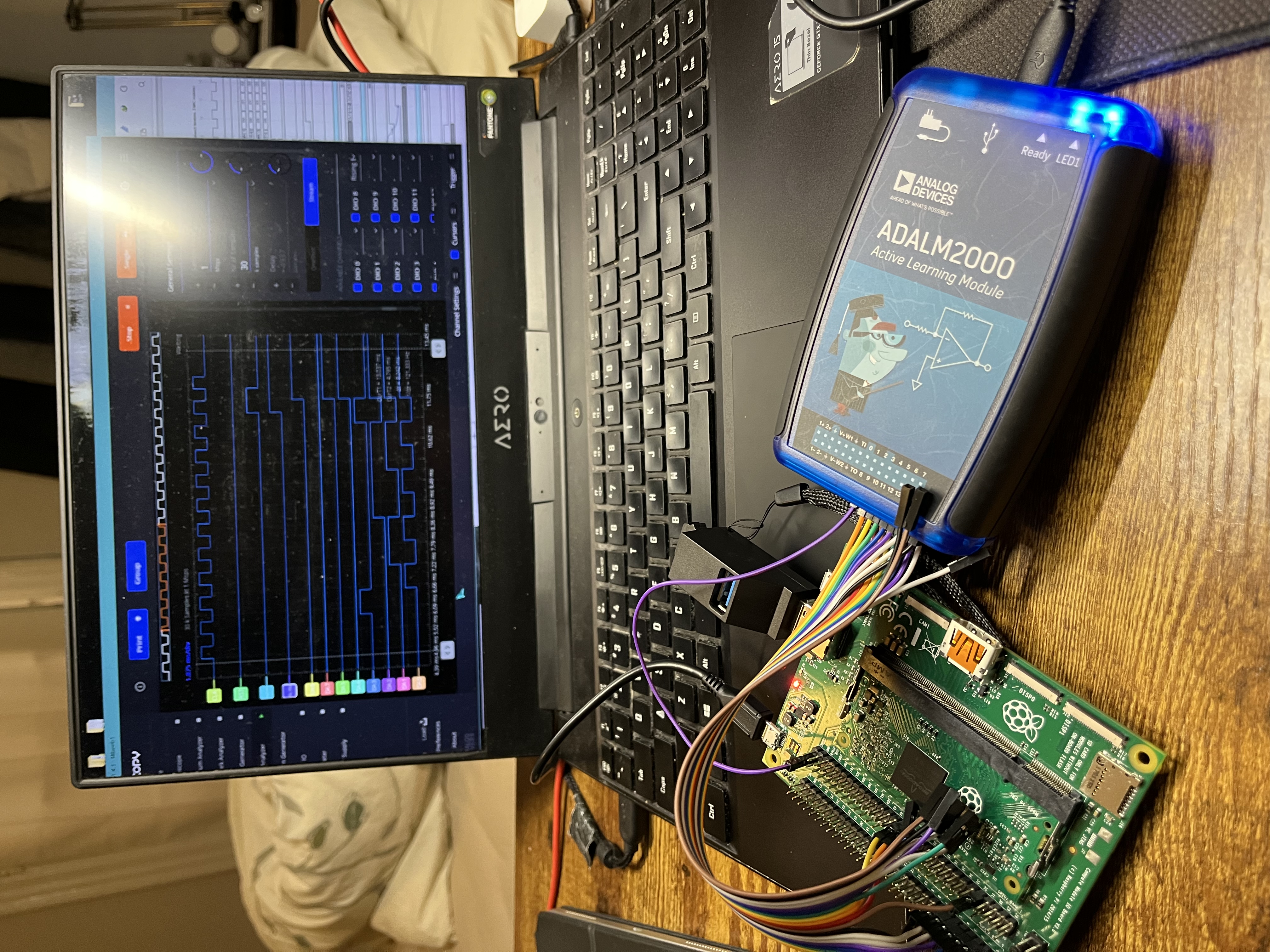
Figure 4. RPI timing measurement setup
After we confirmed the outputs from RPI are correct, we connected RPI to a FPGA board for an emulated validation. We programmed that FPGA using the same RTL as our NPU chip to fully emulate its performance and debug RPI code. The setup is shown in Figure 5. We refined our C code in RPI using this emulated setup and made sure the host system is fully prepared for the PCB with NPU. This is also a good approach to isolate two systems first and make sure one of them is bugless.
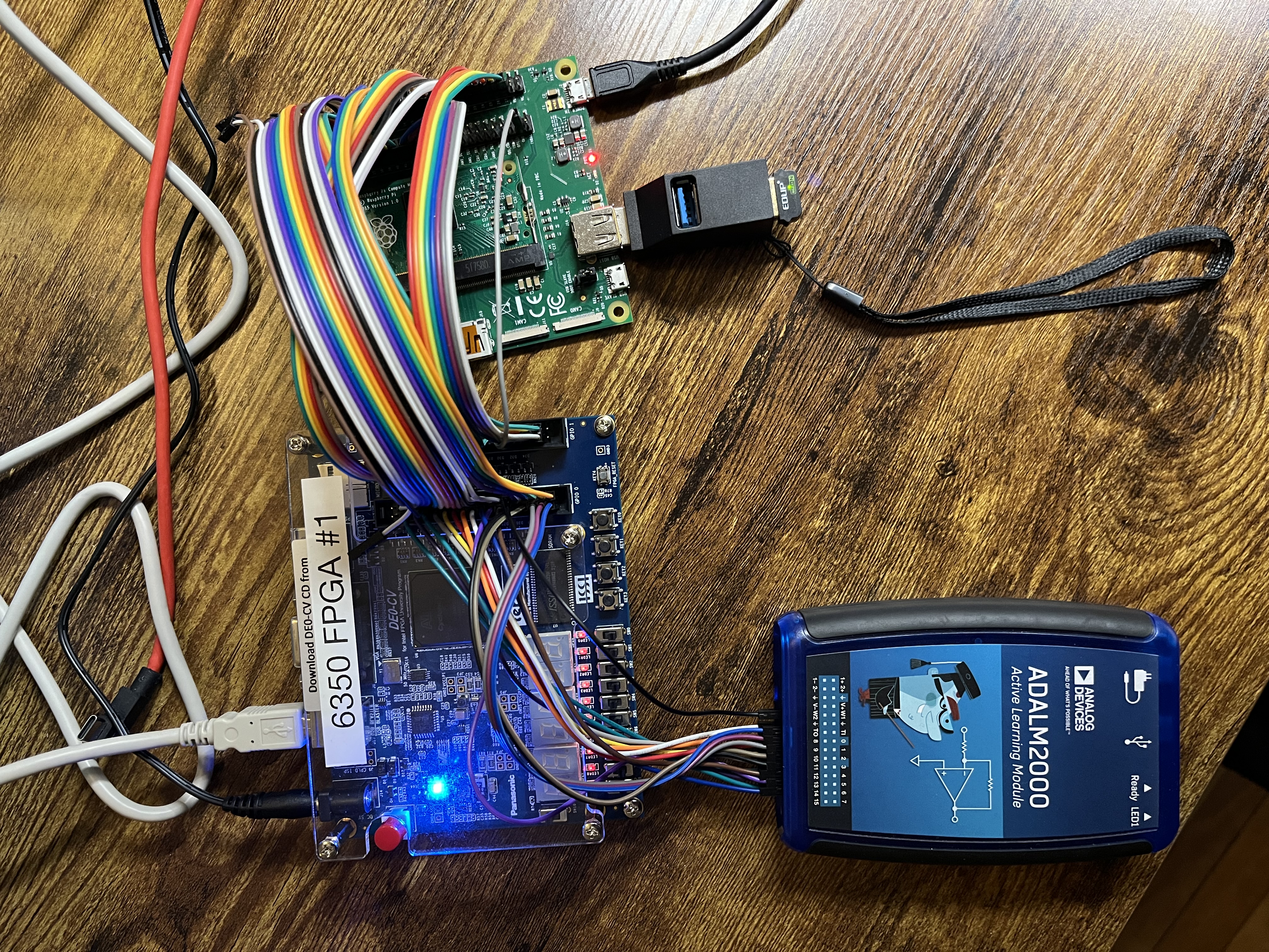
Figure 5. Full system using FPGA for emulated NPU
3D Printed Case & Complete System
Once fully correct results can be obtained from RPI + FPGA emulation, we plugged our NPU PCB onto the RPI headers and validated our chip. We were very fortunate that our chip was fully functional at the first time it was powered on. We achieved a clean connection between two boards by using the same female headers on PCB. This will create a stack of boards as shown in Figure 6.
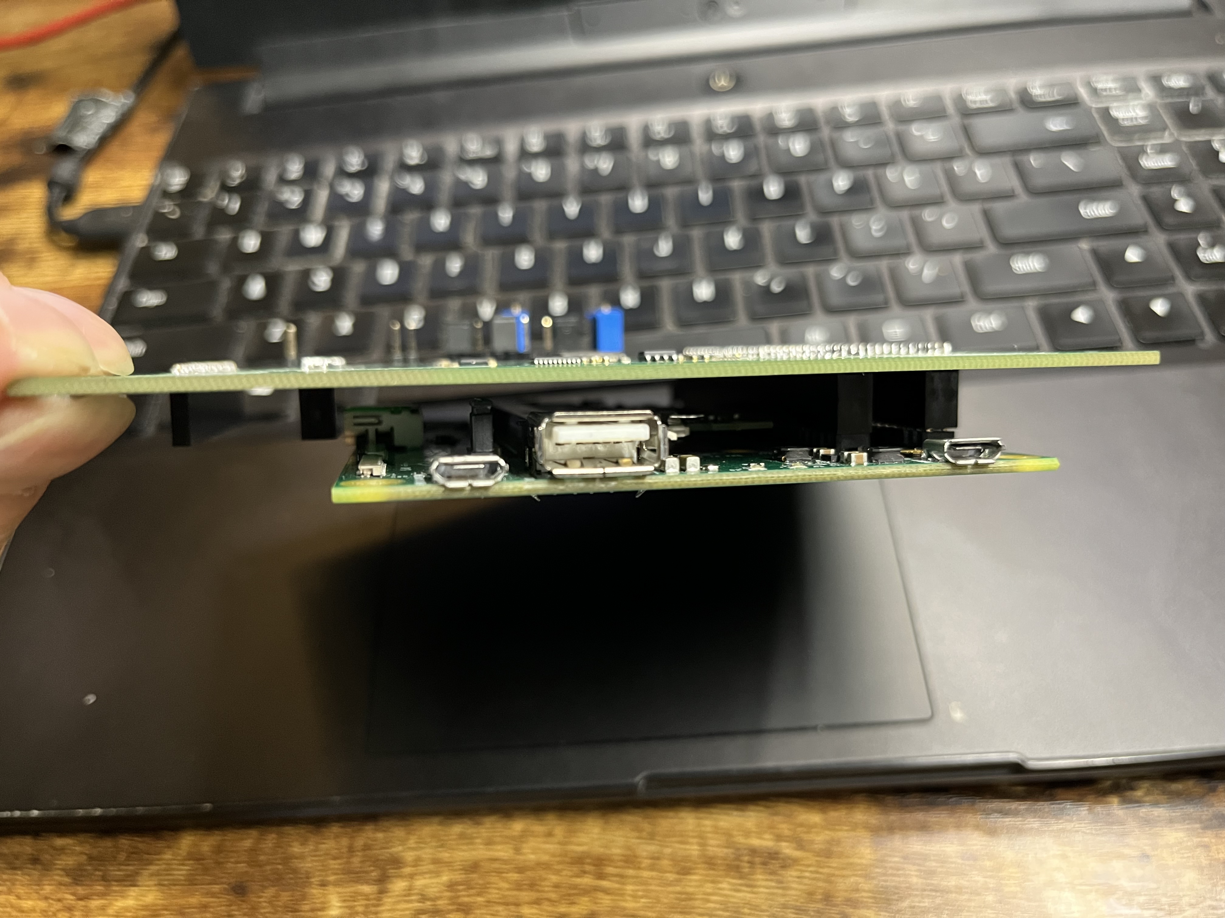
Figure 6. System Stack
We also designed a fancy wrapper for the system, a 3D printed enclosure as mentioned before. The enclosure has space for a power bank, our board stack and a PC camera, thus forming a standalone, self-powered, integrated system. We used this enclosure for the final demo session and the results were great. Figure 7 and 8 included more details about this enclosure, and as we promised, we had a pineapple on top of the case for consistency :)

Figure 7. Case with lid open
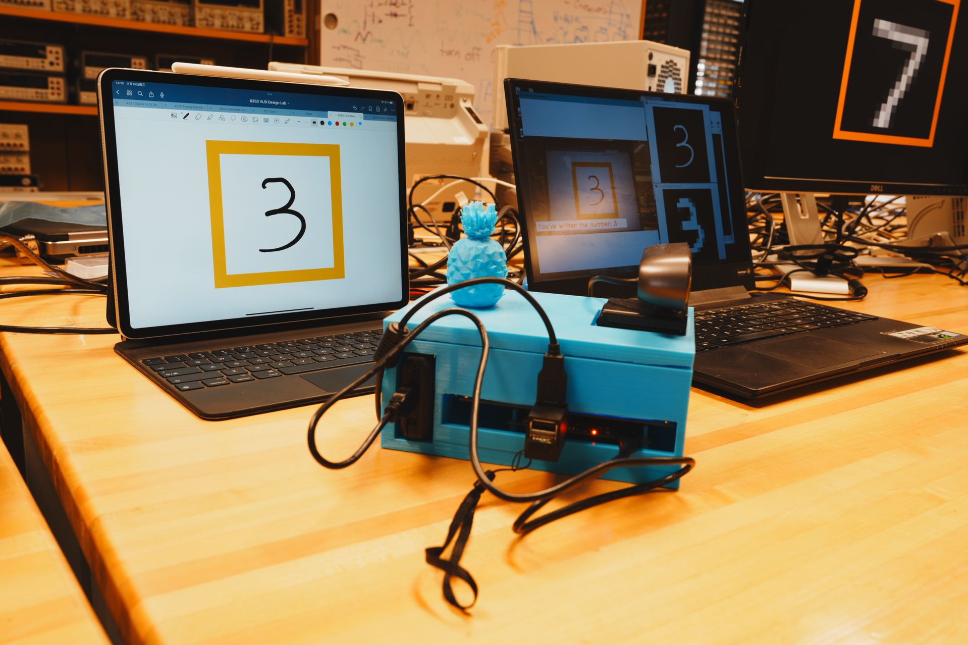
Figure 8. Complete system with boards, power bank and camera
Signal Processing Algorithm
Once we capture a raw image, we need to pre-process the image before it can be pushed into NPU for computation. The signal processing path can be summarized using Figure 9. We showed the results after each processing stage in Figure 10, in which left one is the raw image, top right one is the captured number section from raw image, bottom right one is the compressed image that is ready for NPU computation.
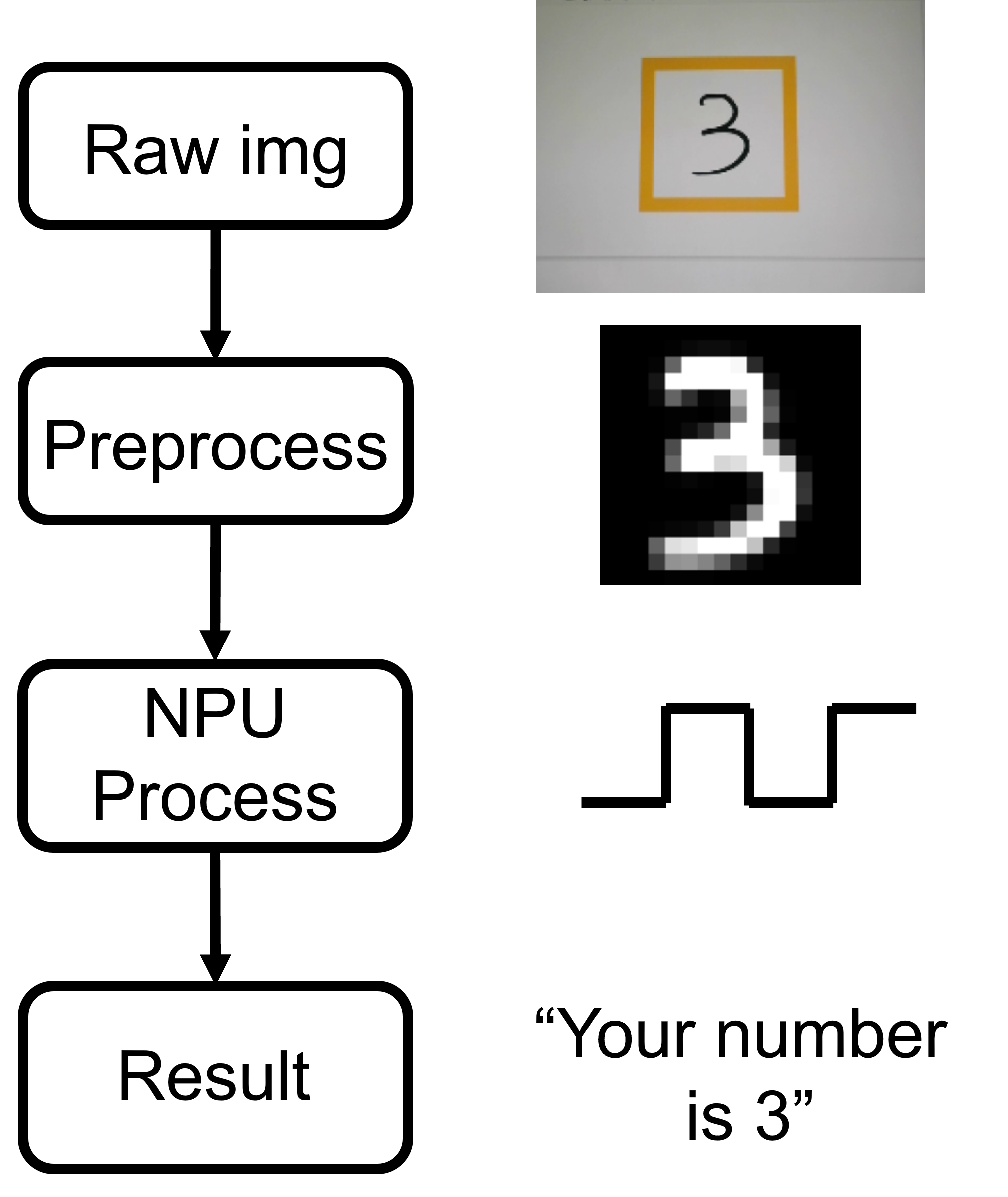
Figure 9. RPI demo siganl processing path
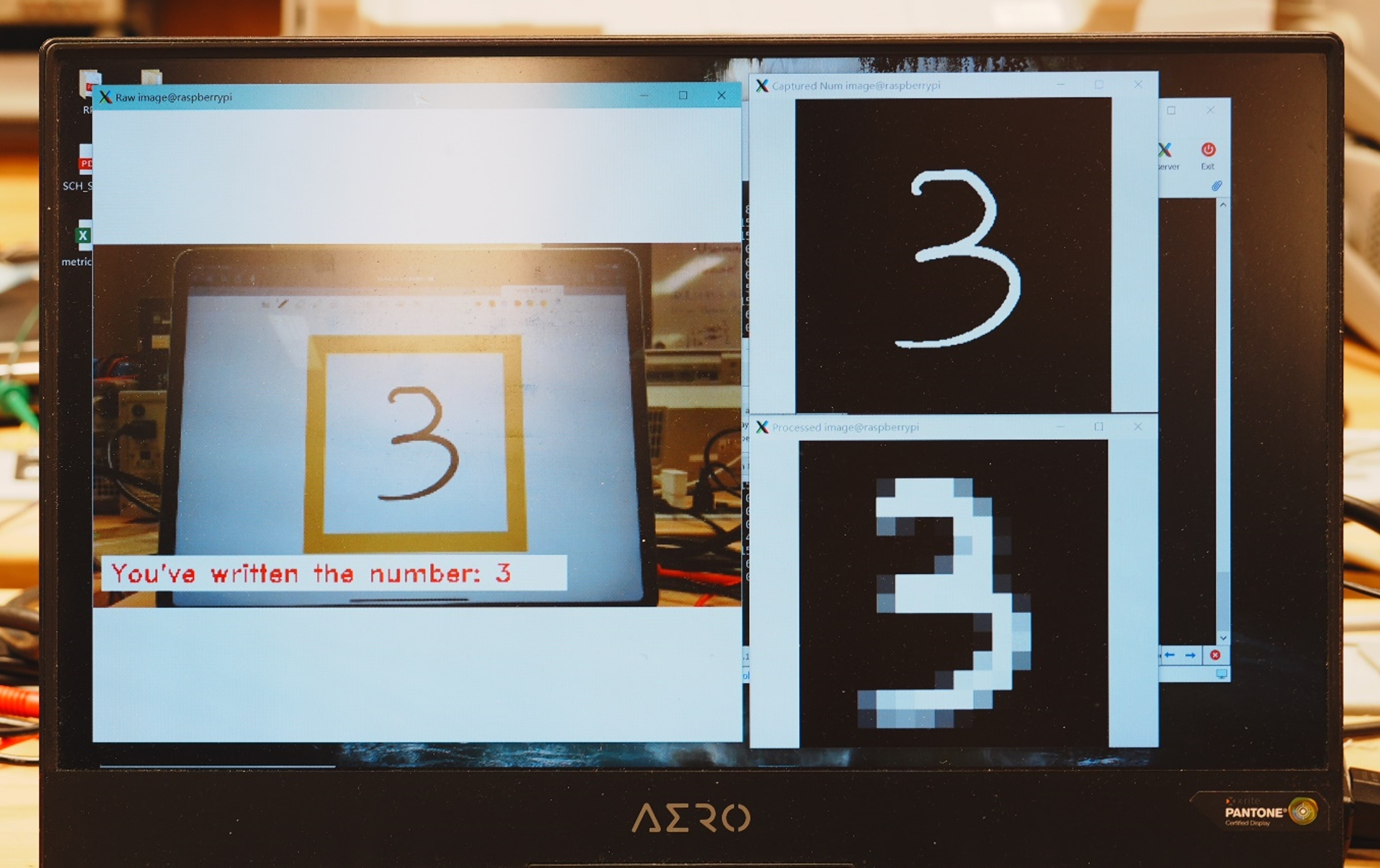
Figure 10. Processed results from different stages
There are two key algorithms in this signal processing path in Figure 9. One is to extract the area bounded by the yellow square that includes the number for processing, the other is to compress this image down to 16 by 16, greyscale format, and improve its similarity to the original MNIST dataset. We used OpenCV and some custom pixel manipulation functions to realize these two algorithms.
For the first algorithm, its logic can be summarized as follows:
- Convert image to HSV Color Space
- Threshold for Yellow Color and extract Yellow Parts
- Convert the yellow parts image to grayscale
- Apply median blur to the greyPic to smooth out noise
- Convert greyPic to a binary image binPic using thresholding
- Use Canny edge detector on binPic to get the edges
- Find contours in cannyPic and draw each detected contour on a blank image linePic
- Find the contour with the maximum area
- Find the convex hull of the maximum area contour
- Sort the vertices of the maximum area contour and map the vertices to a rectangle in the output image
- Compute the perspective transform matrix and apply the perspective transform on srcPic
Essentially what it does is locating the corners of the yellow square and capturing the image within this square. It then conducts a series of processing to clean the noise, transforms the image based on thresholding and calibrates the angle using perspective transform. There is solid math behind this typical CV algorithm, please refer to OpenCV library for more information. This algorithm will transform the raw image in Figure 10 to top right image.
For the second algorithm, its logic can be summarized as follows:
- Blur the binary image using Gaussian blur
- Gradually size the image to 28x28
- Increase the contrast
- Remove surrounding black pixels, normalize, then add paddings to 28x28
- Match the mass center with image center
- Resize the image to final width of 16x16
- Increase image contrast again
This algorithm mainly focuses on downsizing and matching image to original MNIST pattern. The step of matching the number mass center with image center is very important, since MNIST use this for all normalization. This will significantly affect the recogntion accuracy. This algorithm will transform the top right image in Figure 10 to bottom right image in Figure 10. Now the image is 16x16 and all pixel values are between 0-255. We further divided everything by 16 so that all pixel values are within 0-16. This will effectively avoid saturation during computation and improve NN stability.