
PCB Design
In order to verify the functionalities of the NPU, we designed a 2-layered PCB using LCEDA. Its top level schematic is as shown in Figure 1. The main purpose of this PCB is to establish connection with either Raspberry Pi or FPGA, therefore its configuration is simple:
- Power Circuitry
- 6* 8-channel level shifter and 1* 2-channel level shifter
- RPI Header (Demo 1)
- FPGA Header (Demo 2)
- NPU
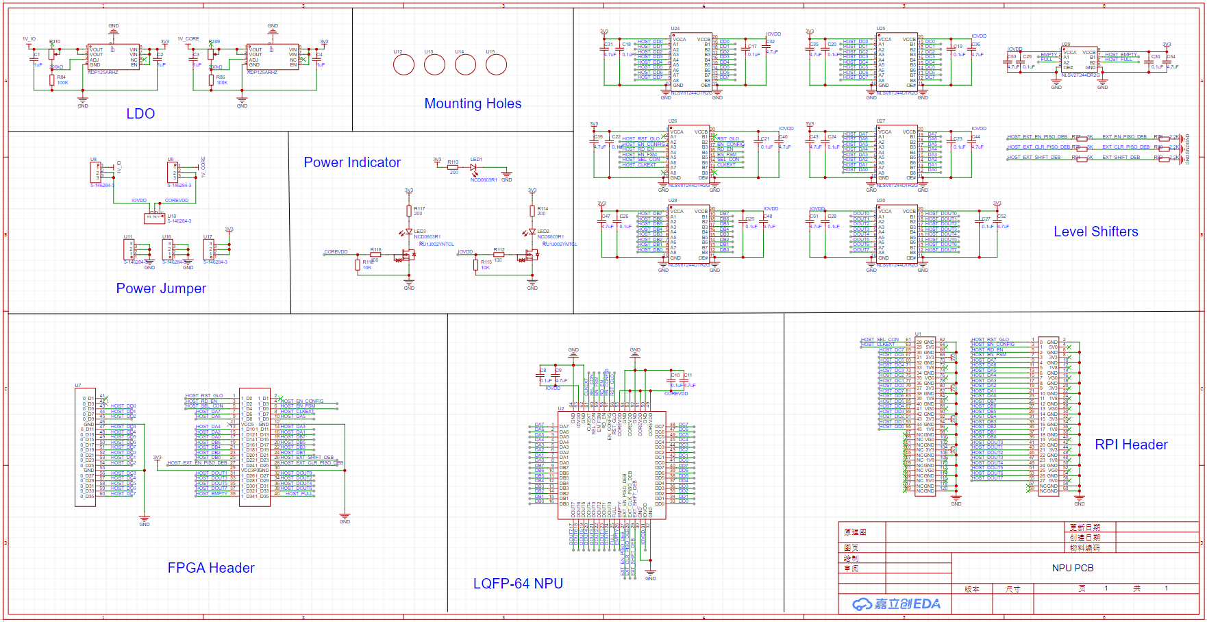
Figure 1. Top-level PCB Schematic
Power Circuitry
The power source of the PCB is either from the RPI IO board or the FPGA, both are 3.3V. The voltage domains of the NPU(both IO_VDD and CORE_VDD), on the other hand, are both 1V. Therefore, we used two identical LDOs to generate 1V_IO and 1V_CORE, as shown in Figure 2. To fine tune the output voltage, and to overclock the NPU when needed, we replaced one of the feedback resistors with a potentiometer.
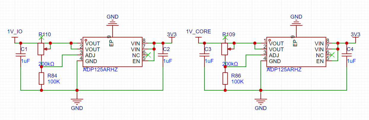
Figure 2. LDOs to generate 1V_IO and 1V_CORE
Ideally, we would like to power the entire NPU with 1 single voltage source, therefore we included three jumper headers to give us the option to join IO_VDD and CORE_VDD, as shown in Figure 3.
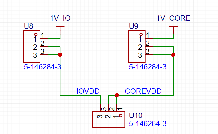
Figure 3. Power Jumper Headers
We also included three blue LEDs as our power indicators, as shown in Figure 4. Since 1V(CORE_VDD and IO_VDD) is less than the forward voltage of the LED, we used a logic level MOSFET as the LED driver.
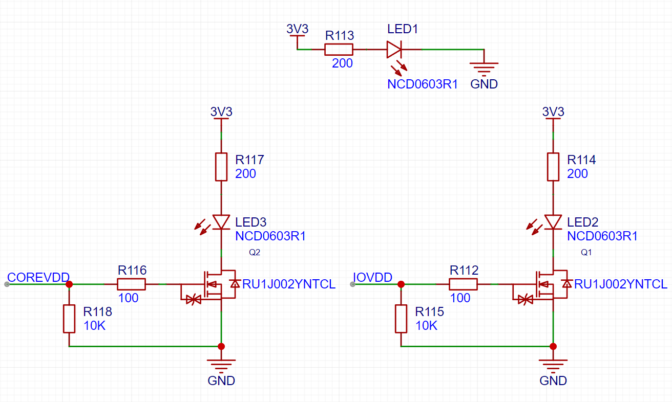
Figure 4. Power Indicators
Level Shifters
We included six 8-channel level shifters and one 2-channel level shifter to down-convert
input signals from 3.3V to 1V, and up-convert output signals from 1V to 3.3V, as shown in
Figure 5. All the level shifters are bidirectional.
For EXT_EN_PISO_DEB, EXT_CLR_PISO_DEB, and EXT_SHIFT_DEB, voltage dividers are used instead,
as the three signals only serve the debugging purpose and they do not require high performance.
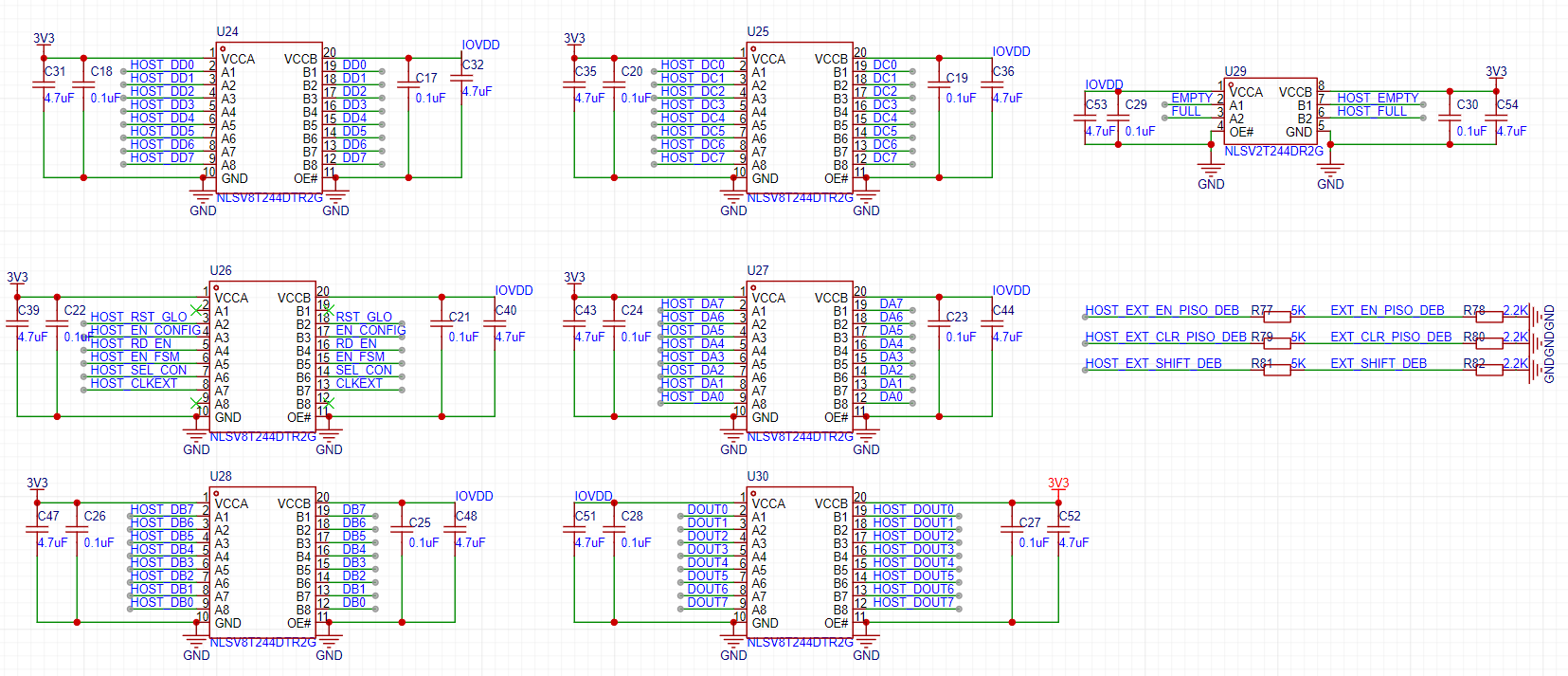
Figure 5. Level Shifters
RPI and FPGA Header
On both the Raspberry Pi IO board and the FPGA board, there are a series of 2.54mm male headers. To avoid using any cables, we designed female headers with the exact dimensions, as shown in Figure 6. In this way, connecting NPU PCB to either RPI IO board or FPGA board is as easy as aligning the female and male headers and applying (significant) force. Pictures showing the connection can be found in Demo 1: RPI+NPU and Demo 2: FPGA+NPU.
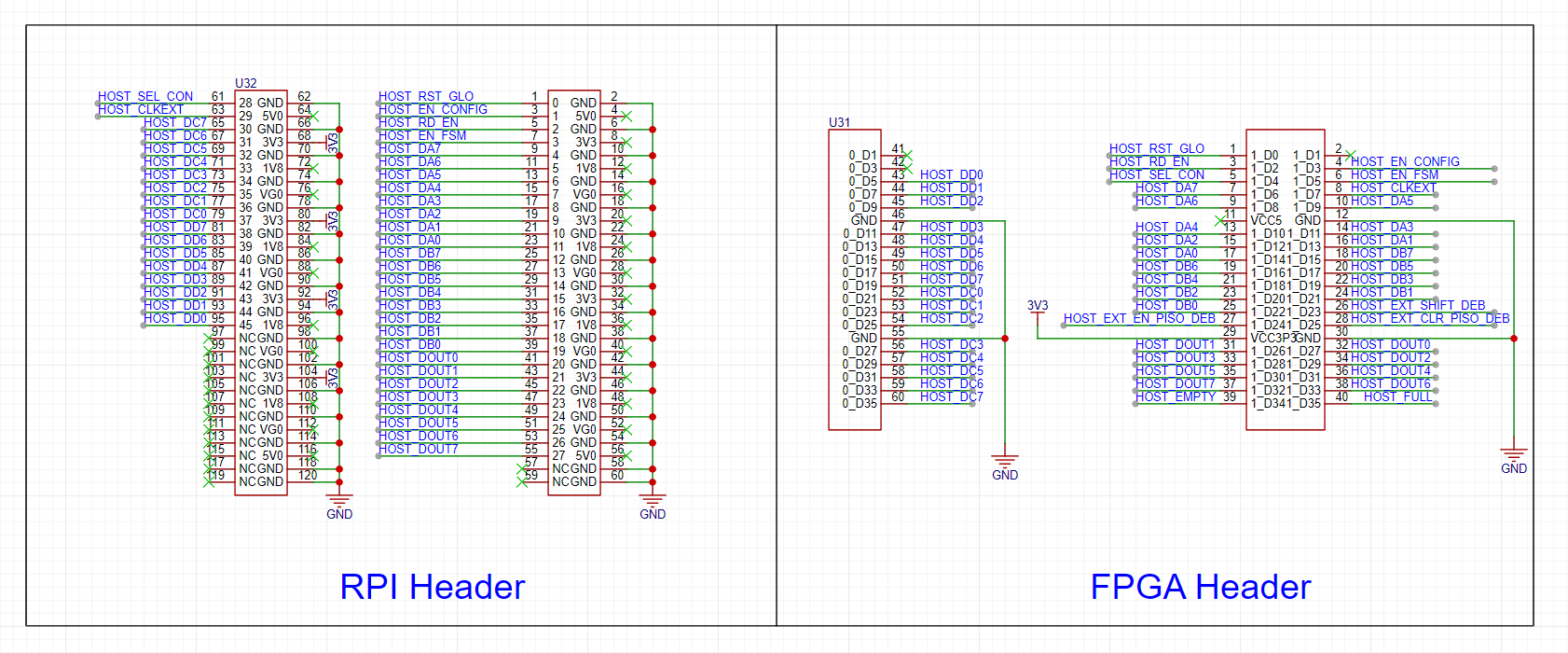
Figure 6. RPI and FPGA Header
PCB Layout
The layout and 2D-preview of the PCB is shown in Figure 7 and Figure 8.
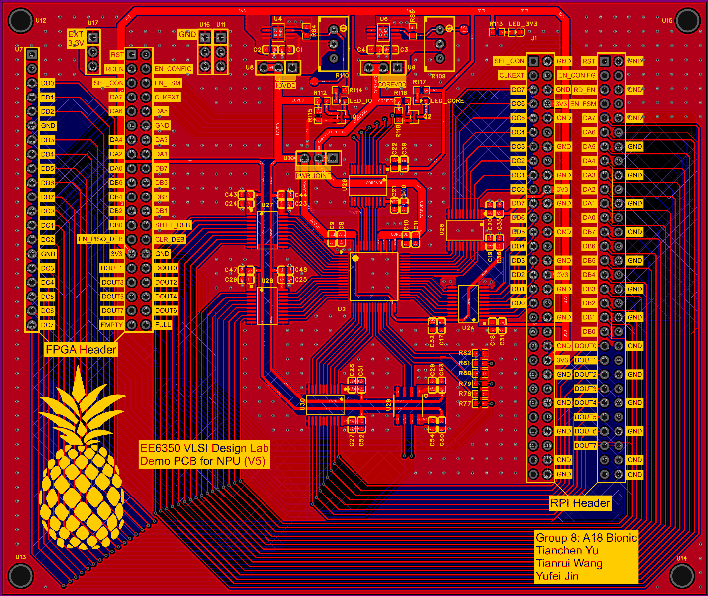
Figure 7. PCB Layout
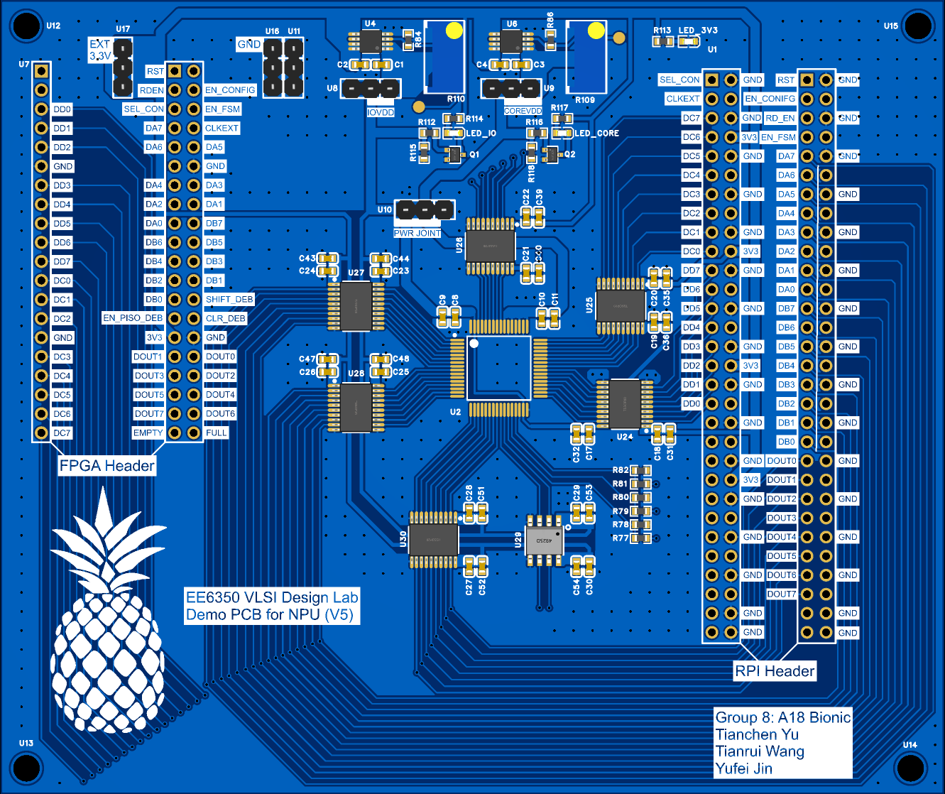
Figure 8. PCB 2D-preview
Soldering
In order to keep the PCB compact, we chose to not use the chip socket. Considering the high difficulty of soldering the several level shifters and the NPU itself, we ordered a stencil from JLCPCB and decided to go with reflow soldering. Figure 9-12 show the steps of utilizing the stencil and getting the PCB ready for the reflow oven.
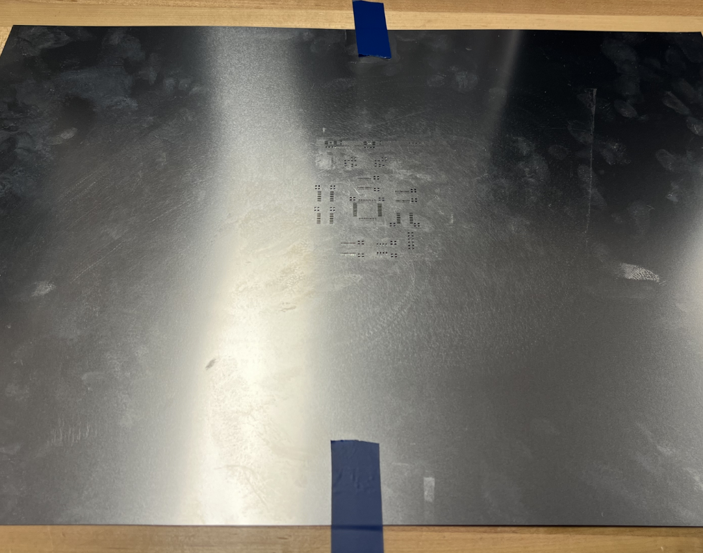
Figure 9. Align the stencil openings with the PCB pads
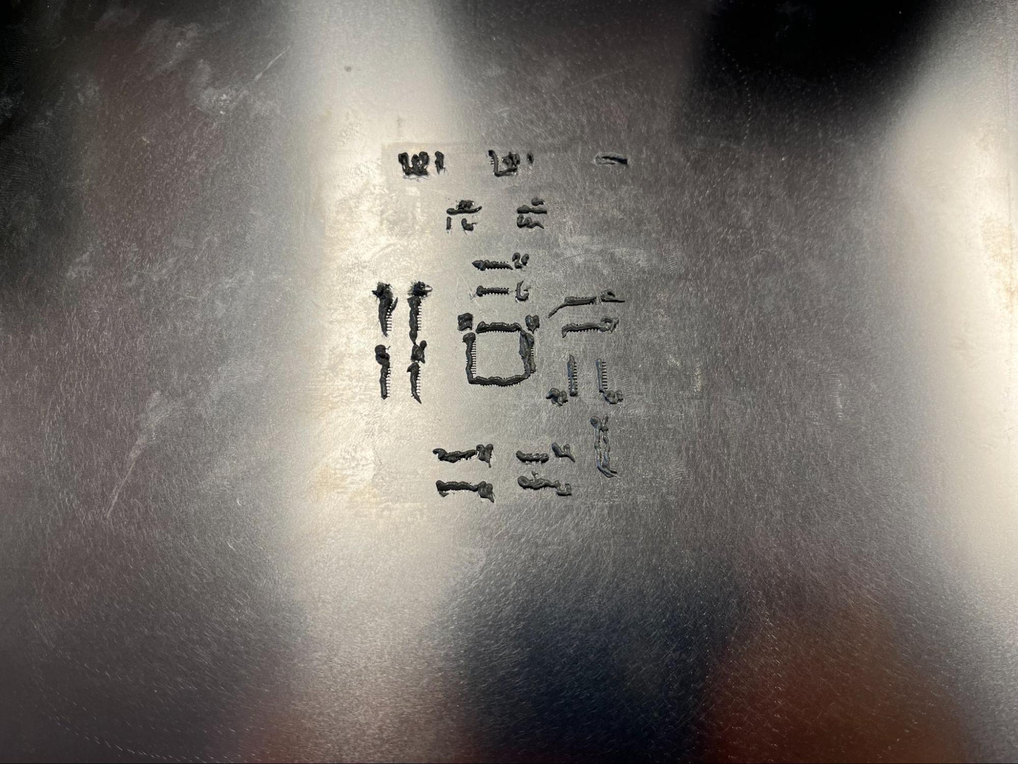
Figure 10. Apply solder paste
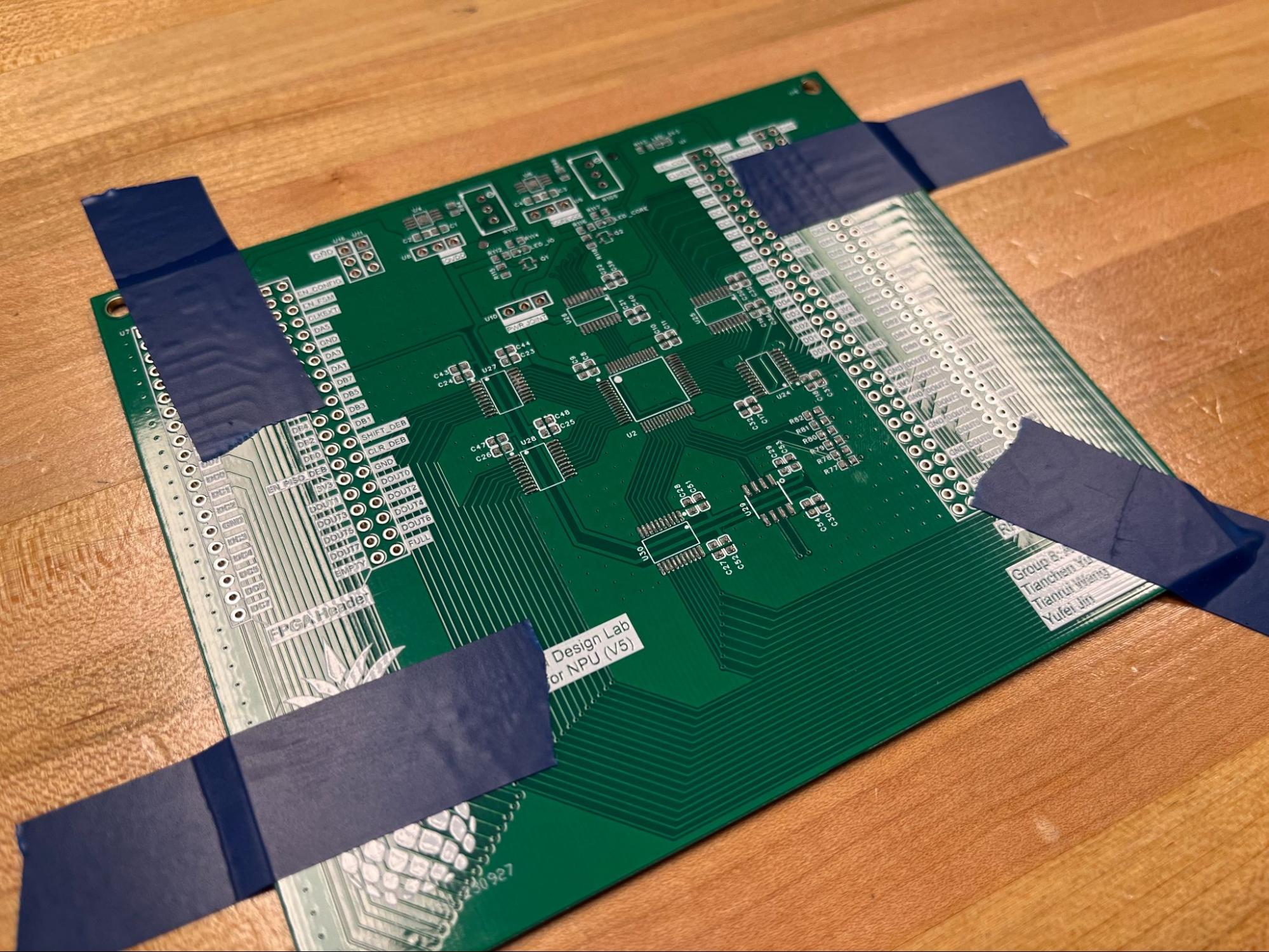
Figure 11. Carefully remove the stencil
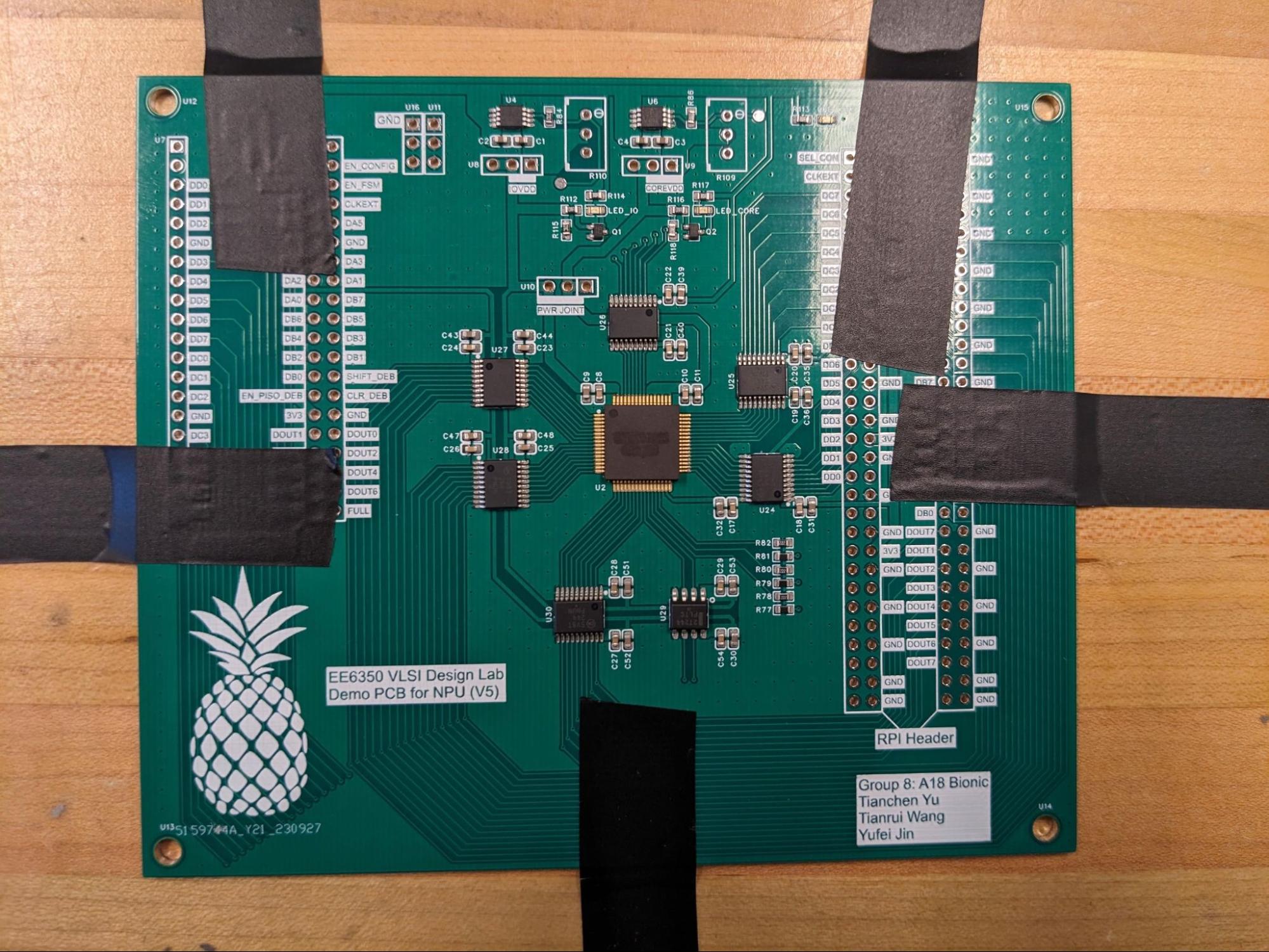
Figure 12. Place the surface mount components on the soldering paste
After this step, the PCB is ready to go into the reflow oven. We then soldered the through-hole components by hand and the assembled PCB is shown in Figure 13.
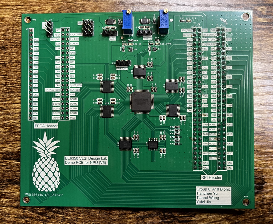
Figure 13. Assembled PCB