
Demo 2: FPGA+NPU
In demo 2, we configured the FPGA to serve as the host of NPU. A detailed block diagram is
shown in Figure 1. The motivation for designing a second demo is to verify that NPU is able
to operate under a much higher clock frequency(the fastest we could get is 6.25 MHz), compared
with the 2 kHz frequency scenario in Demo 1: RPI+NPU.
As mentioned in Verification, we reprogrammed the Verilog testbench(TEST 5) as
synthesizable RTL code, which we called the scheduler. The scheduler keeps an internal
counter, and we specify the NPU's input/control signals for each counter value.
We also hard programmed the weights and biases of the neural network(param reg) and four
images(image reg) into the FPGA, and connected a monitor to display the current image under
inference. A 7-segment display on the FPGA board prints the recognition result of the current image.
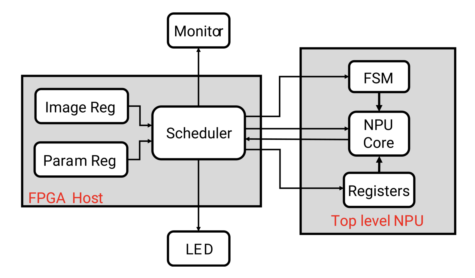
Figure 1. Demo 2 block diagram
The FPGA host is connected to the NPU through the male headers on the right of Figure 2. As mentioned in PCB Design, the PCB board for the NPU has matching female headers, allowing for a direct plug in.
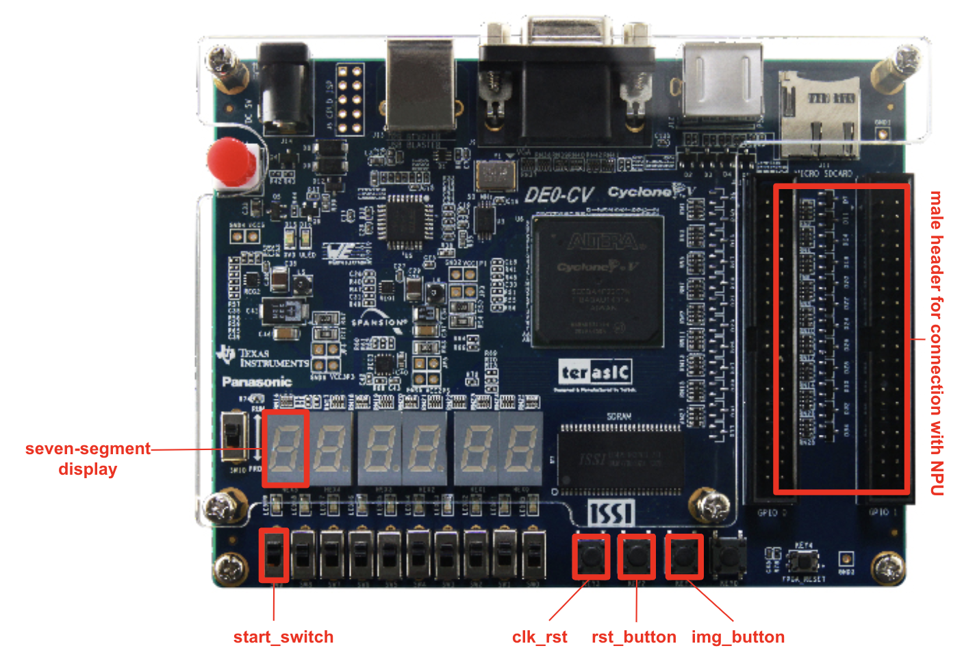
Figure 2. FPGA board programmed switches and buttons
We programmed 3 buttons and 1 switch on the FPGA board for demo 2.
The first button is called clk_rst. As the FPGA board runs at 50 MHz
and the NPU runs at a much lower frequency, a clock divider
module is included in the FPGA program to help provide clock for the
NPU, which depends on the clk_rst signal to initiate and synchronize.
The rst_button resets the internal counter of the scheduler. It restarts
the inference process on the current image. This button comes in handy
when we try to probe signals out of the system with a logic analyzer.
The img_button helps switch to and start the inference process on the
next image. When the four images are exhausted, it returns to the first
image in image reg.
The start_switch enables the inference process. If start_switch is 0 the
internal counter of the scheduler resets to and stays at 0.
Typical sequence of demo 2 is to push clk_rst first, rst_button second,
and then flip the start_switch. This is when we will see the seven-segment display showing the first recognition result. Then pressing img_button would help us verify the prediction of the following images.
The actual connection of the FPGA board and NPU PCB is shown in Figure 3. The entire demo view
is shown in Figure 4. In Figure 4, the monitor is displaying the image under processing, and the 7-segment
LED is showing the recognition result. In this case the image is a hand-written seven and the LED is showing
the current result.
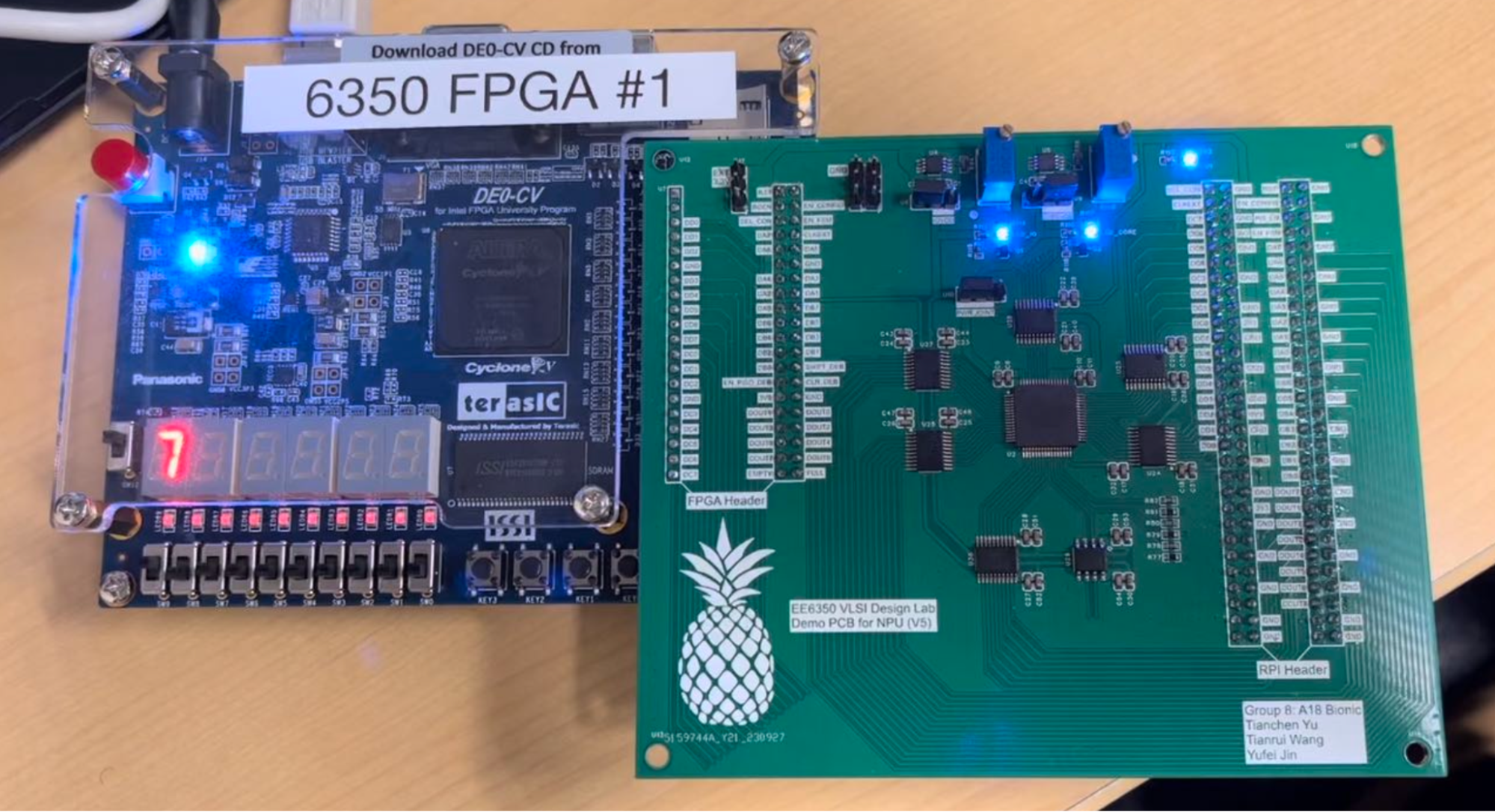
Figure 3. NPU PCB - FPGA board connection through direct plug in
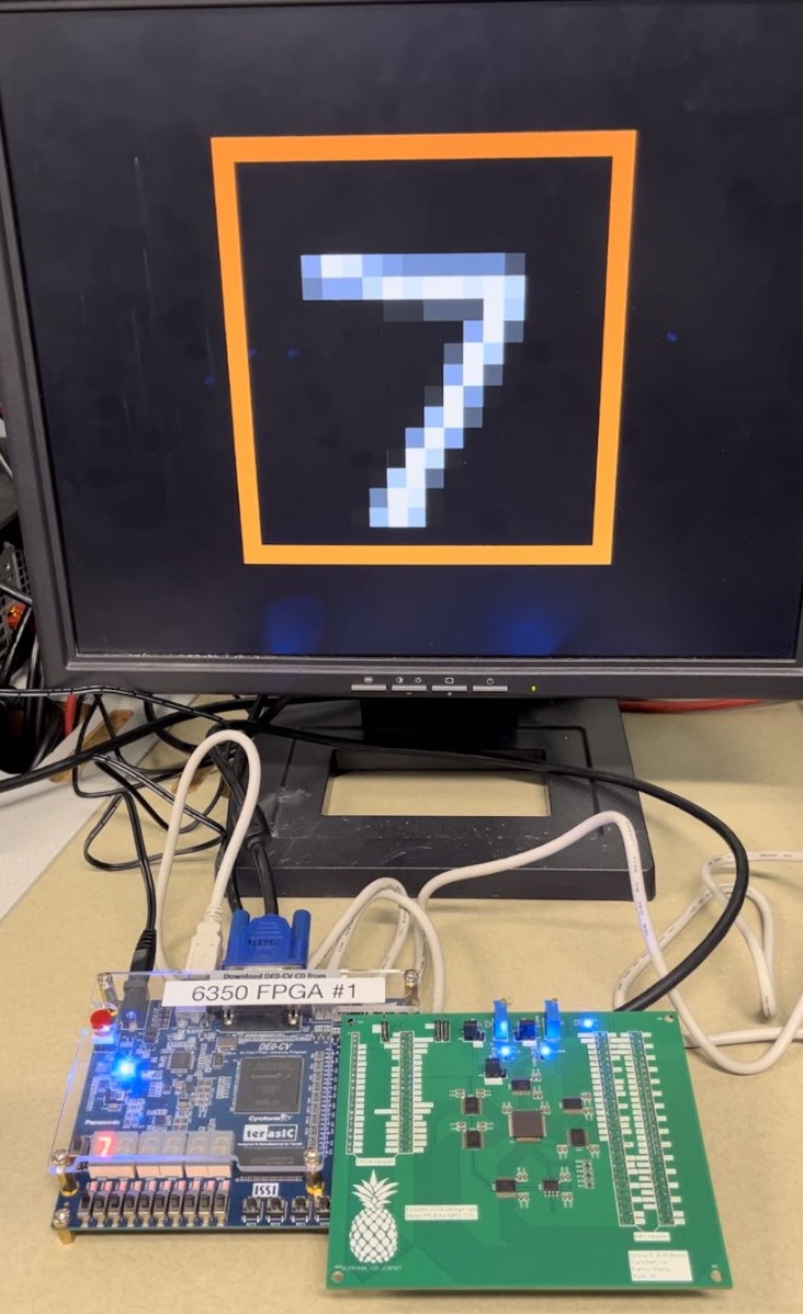
Figure 4. Entire demo 2 setup
We also find it interesting(and to exonerate ourselves from cheating) to look at the logic analyzer results, with which we probed four signals. The results are shown in Figure 5.
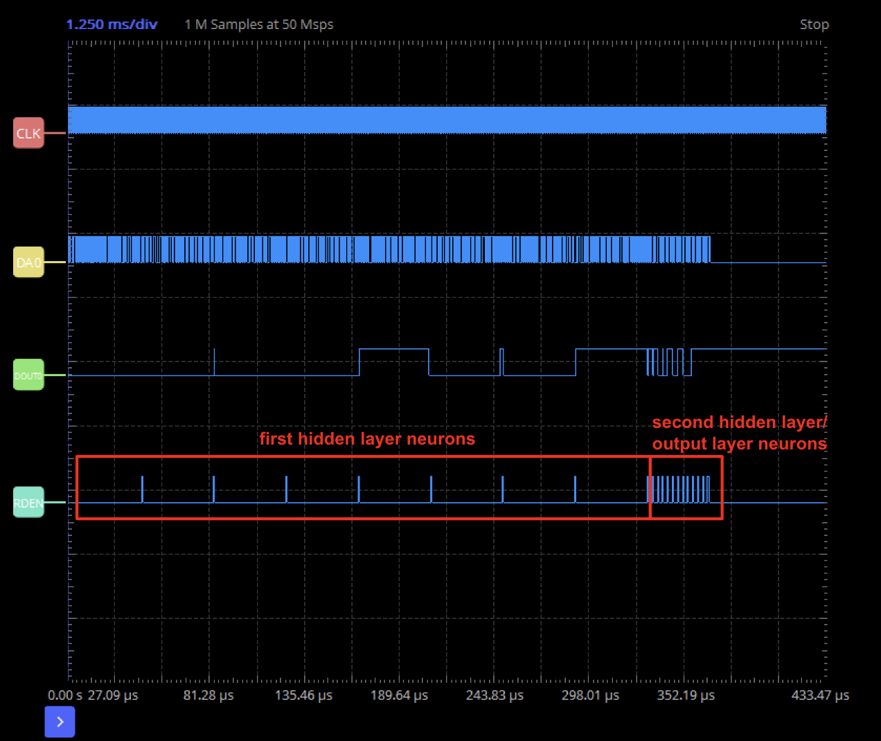
Figure 5. Logic analyzer results
The four signals, from top to bottom, are the NPU clock, DA0(one of the
input), DOUT0(one of the output), and RD_EN, which is a control signal.
RD_EN is used to control the output FIFO, and in the scheduler we pull
RD_EN high each time two neurons are ready(as we have two pipelines).
Therefore, we can easily see that computing two neurons takes a longer
time in the beginning, and becomes very fast towards the end. This is
due to the structure of our neural network. To compute the 16 first
hidden layer neurons, as we have 256 input neurons, it would require
256 MAC operations, and therefore around 256 cycles between each RD_EN
high. For the second hidden layer, the inputs are the 16 first hidden
layer neurons, and therefore around 16 cycles between each RD_EN high,
and the same goes for the output layer.
Comments:
We spent some time debugging the scheduler Verilog code for synthesis.
As we managed the posedge and negedge blocks separately, we included
some signals both in the posedge and negedge, resulting in a multiple
driver issue. The multiple driver issue is considered a warning instead
of an error in Genus, and our code involves a lot of other operations that
could potentially go wrong, like multiple array packing and unpacking,
and array muxes. Therefore it took us days to identify this multiple driver
issue.
When we tried to synthesize the code using Quartus, another problem
got in the way. Apparently our scheduler module was too complex and
could not be synthesized, so we had to split this module into two
modules.
Although we synthesized the NPU core at 100 MHz, we were only able to
clock it at 6.25 MHz(1/8 of the FPGA clock). We suspected that this
problem is due to the very large VDD ringing on the PCB.