

Layout
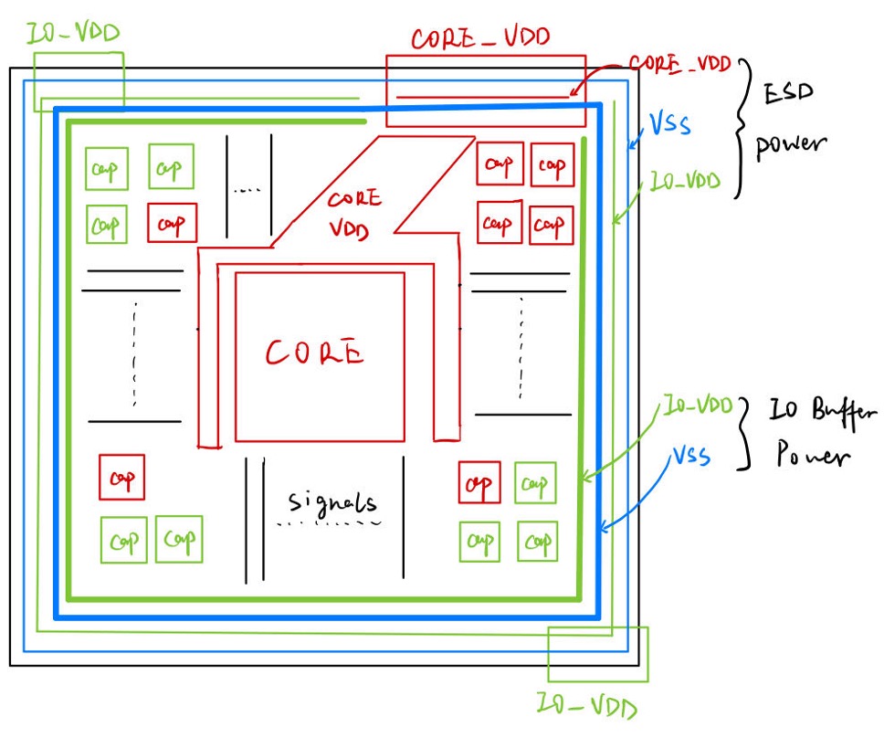
Figure 1. NPU Layout floor plan
Figure 1 illustrates the layout floor plan of the circuit. In this design, the input buffers were placed adjacent to the input pins, the output buffers were placed next to the output pins, and the Schmitt trigger is positioned close to the clock pin.
The design incorporates two voltage domains, both operating at 1V. The first domain, CORE_VDD, consists of four pins. These are connected to the VDD of the digital core. All CORE_VDDs are grouped together. The second domain, IO_VDD, has two pins. This domain is responsible for powering all IO buffers and the Schmitt Trigger, along with their associated ESD protection circuits. In this design, the IO_VDD pins are divided into two groups, each located at a corner of the layout. This symmetrical arrangement likely serves to balance the power distribution and to minimize potential interference or signal integrity issues across the circuit.
In this project, we interact with Cadence Innovus using TCL scripts provided by Rui Xu to generate the layout for the NPU core. The script `1_import.tcl` is used for environment setup, design initialization, reading design files, and setting up power and ground connections. The `2_floorplan.tcl` script includes key steps such as creating the floorplan, reading I/O files, power routing, special routing, and Design Rule Checking (DRC). In `3_place.tcl`, clock gating, reordering of scan chains, and other settings are configured, and the `place_opt_design` command is used for layout optimization. `4_cts.tcl` involves setting up CTS configurations, generating the clock tree, and post-CTS timing optimization. `5_route.tcl` sets various global routing parameters, such as the design's bottom and top routing layers, routing strategies (like timing-driven and signal integrity-driven), and detailed routing parameters. `6_checks.tcl` includes parasitic extraction, timing analysis, DRC, and several other verification steps. Finally, post-layout netlists and parasitics are exported through `7_export.tcl`.
The Worst Negative Slack (WNS) of our design in setup mode is reported as 0.908ns for both 'all' and 'default' scenarios, and slightly higher at 1.031ns for 'reg2reg'. The Total Negative Slack (TNS) is 0.000ns across all scenarios, indicating no cumulative timing violations. Furthermore, there are no violating paths reported in any scenario, with the total number of paths analyzed being 3524.
In terms of Design Rule Violations (DRVs), the report shows no violations in maximum capacitance, transition, fanout, and length across all nets, as indicated by zeroes in the number of nets (and terms) affected and the worst violation for each category.
The density of the design is relatively moderate at 27.904%, which reaches a complete 100.000% when including fillers. Additionally, the report notes the absence of any glitch violations.
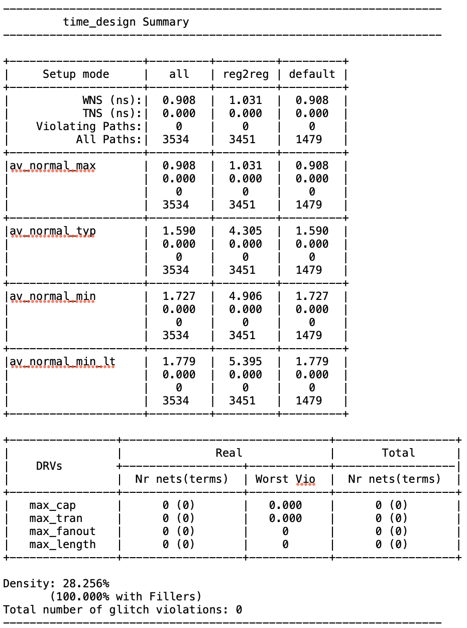
Figure 2. Sign off setup mode report
In terms of hold mode, there are zero violating paths reported in all scenarios, signifying that the design meets the hold time requirements. Consistently, the TNS is reported as 0.000ns across all modes and views, indicating no cumulative hold timing violations.
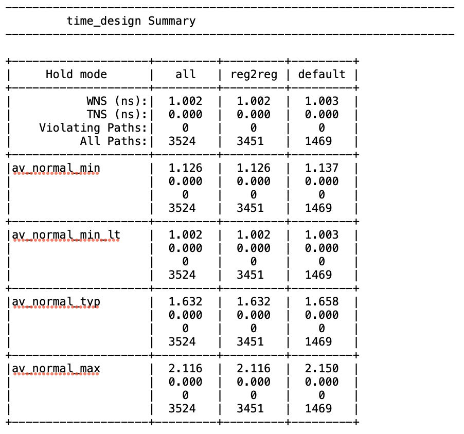
Figure 3. Sign off hold mode report
The NPU core are laid out using metal layers M1 to M3, the signal lines are laid out using metal layers M4 to M7, and the power lines utilize metal layers M8 and M9, providing robust and reliable power distribution to the entire circuit. The design strategically separates signal and power lines, placing them on different metal layers without overlap. This arrangement significantly minimizes interference, ensuring clearer signal transmission and more stable power distribution throughout the circuit. Also, decoupling capacitors are maximally placed at each of the four corners.
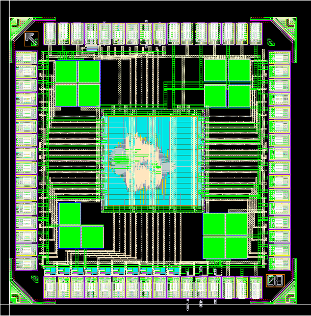
Figure 4. NPU Layout