
Introduction
Welcome to the home page of the Trollstigen Open-Source Field Programmable Gate Array (FPGA) project. Please feel free to use the navigation bar above to learn more about the project.
This project was in fulfillment of the Spring 2016 Columbia University courses VLSI Design Lab (E6350), taught by Professor Peter Kinget, and Advanced Digital VLSI Circuits, taught by Professor Mingoo Seok.
The VLSI Design Lab course primarily focused on exposing students to the entire IC design flow. Under close supervision, students perform all the steps of the IC development process: defining the application and specifications of the IC, system and transistor level simulations, layout, parasitic extraction and post-layout simulation, tapeout, and experimental verification of the fabricated IC. The Advanced Digital VLSI Circuits course primarily focused on exposing students to the digital IC design flow. In this course, students perform all the steps of the digital design flow: defining high-level behavioral models, logic synthesis, functional verification, automatic place and route, timing and power analysis, and back annotation and verification. Our project was made possible by the MOSIS Educational Program, which facilitated the fabrication of our IC, and the Electrical Engineering Dept. for their support in the development and testing of our chip.
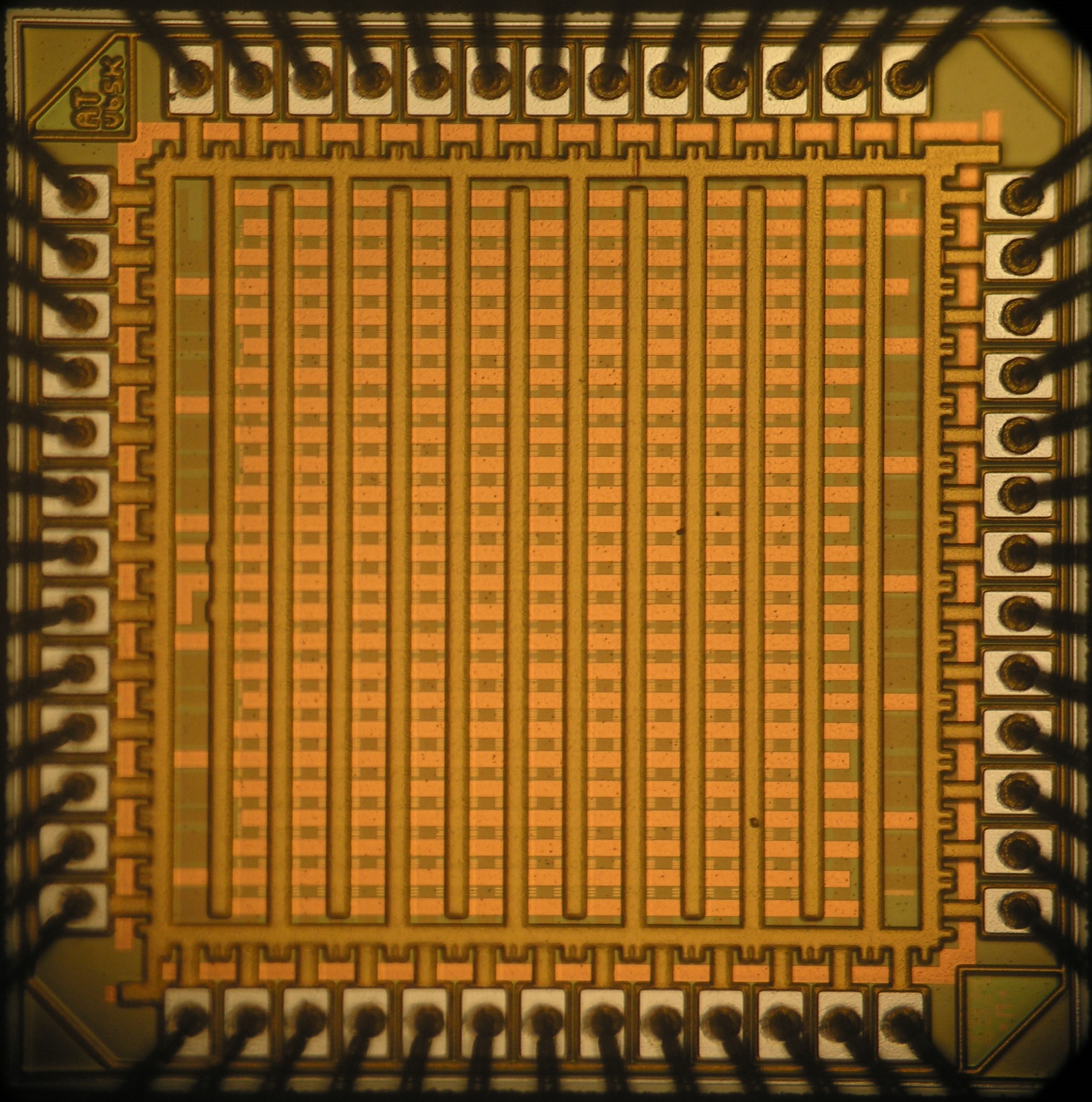
There were numerous motivations behind designing this FPGA. First, we wanted to simultaneously apply the design flows taught in both courses in order to integrate fully and semi-custom circuits in a single package. Second, some of our team members had prior industry experience with FPGAs, and thus wanted to obtain a deeper understanding of the fundamental FPGA architecture and the processes by which software is translated down to the logic block level. Third, we wanted to utilize and expand upon the open-source Verilog to Routing tool to design a real, physically realized FPGA. Finally, we wanted to open-source the software and the hardware, hoping that the academic and hobbyist communities can apply what we have learned.
The software is released on the trollstigen-fpga Github repository. It includes the FPGA Chisel model, bitfile generation tools, and FPGA programming tools.
The demonstration board is released on the Trollstigen FPGA Demo Board Circuitmaker repository. It contains the schematics and layout of the demoboard PCB.
As the IBM 130nm node on which the die was developed is proprietary and subject to NDA, we are unable to release the transistor-level schematics and layout files.