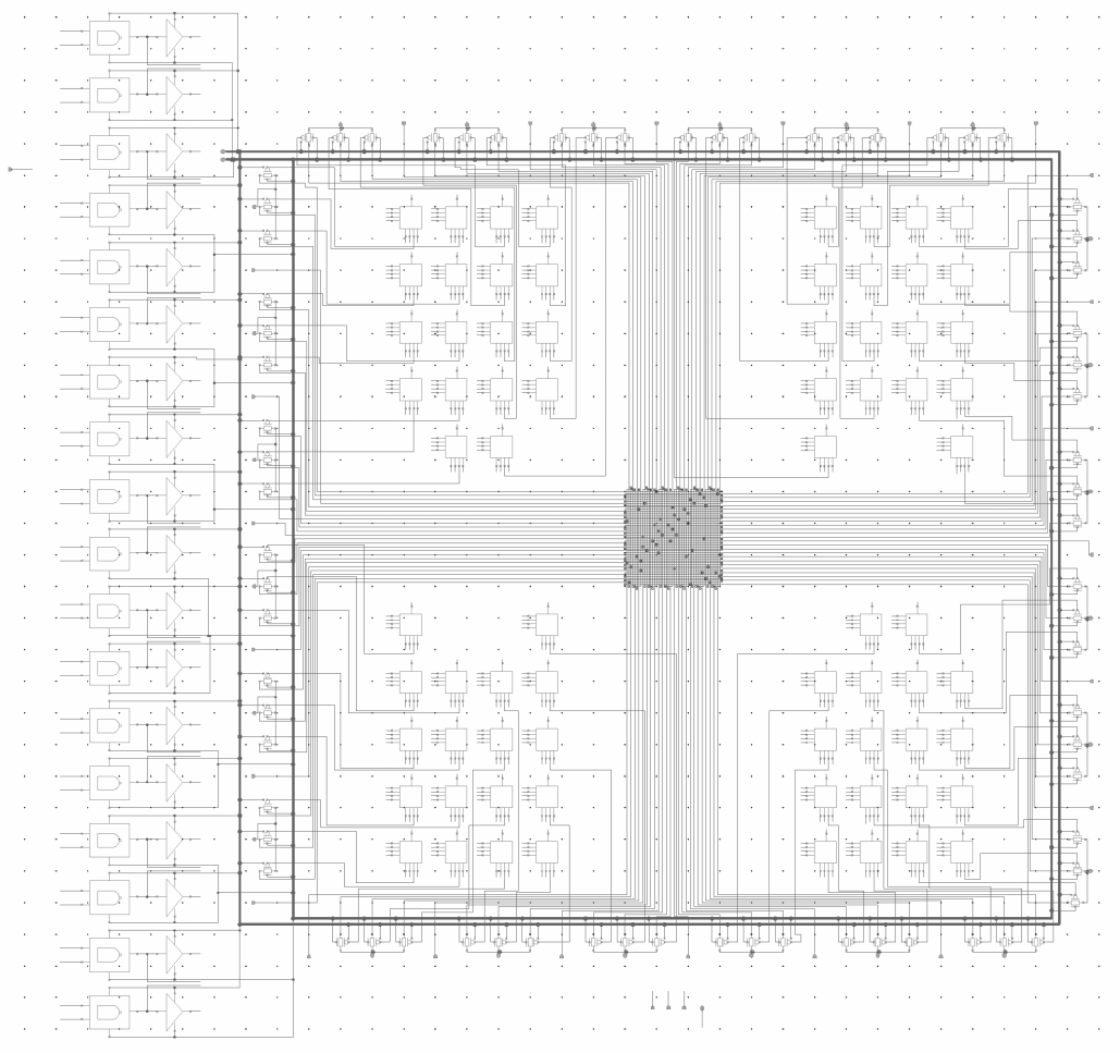
IC Design
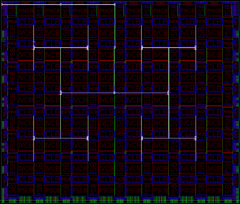
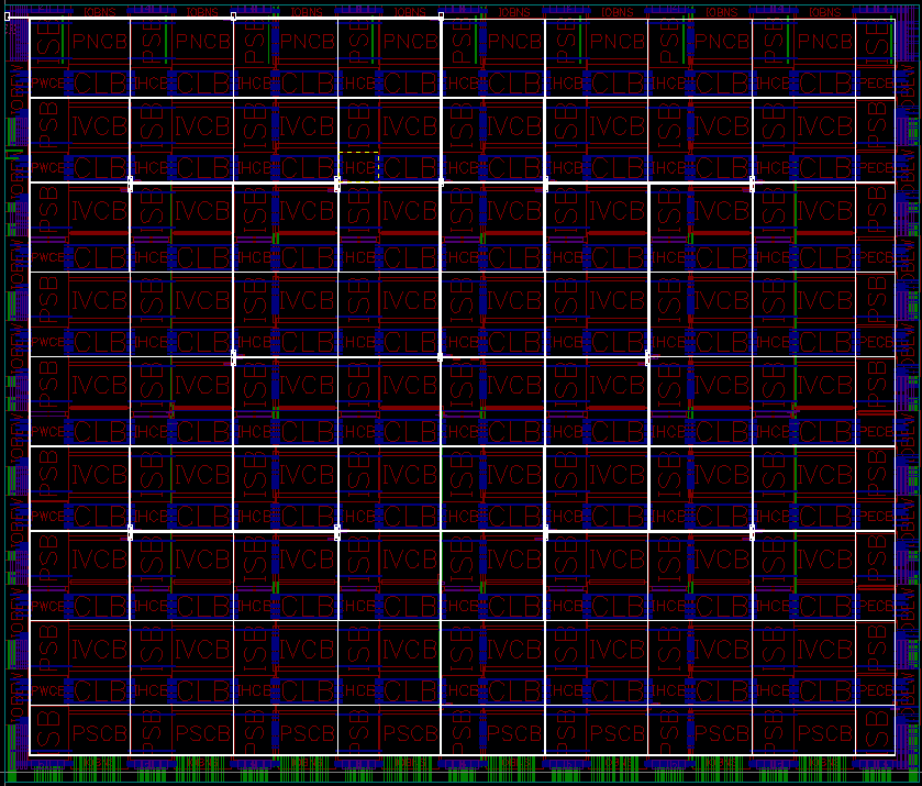
Trollstigen has 8X8 array of tiles with 16 GPIOs+8 HIP ports. The chip also integrated level conversion circuitry (1.2V core<->3.3V I/O) into IO blocks.Verilog is synthesized to bitstream from software flow developed by us through FPGA's asynchronus 8-bit parallel bus. Configuration data is stored in distributed 8X8 cell blocks.
FPGA block level architecture
Level Converters & Output Driver
The level converter has the feature of no contention and fast voltage level convertion with 24mA drive strength with low output impedance [2][3]. Furthermore, a bus keeper is added into the design.
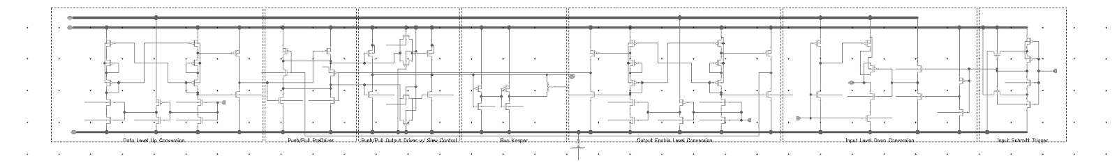
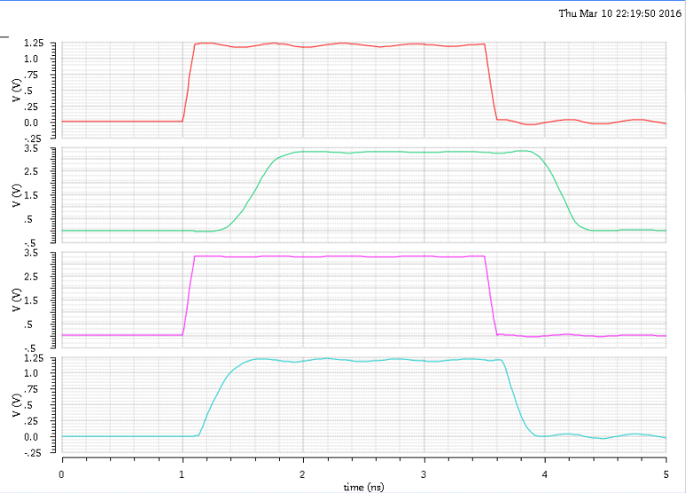
The level converter has approximately 50fF loading. Level up-conversion has approximately 600ps of delay and level down-conversion has 200ps of delay.
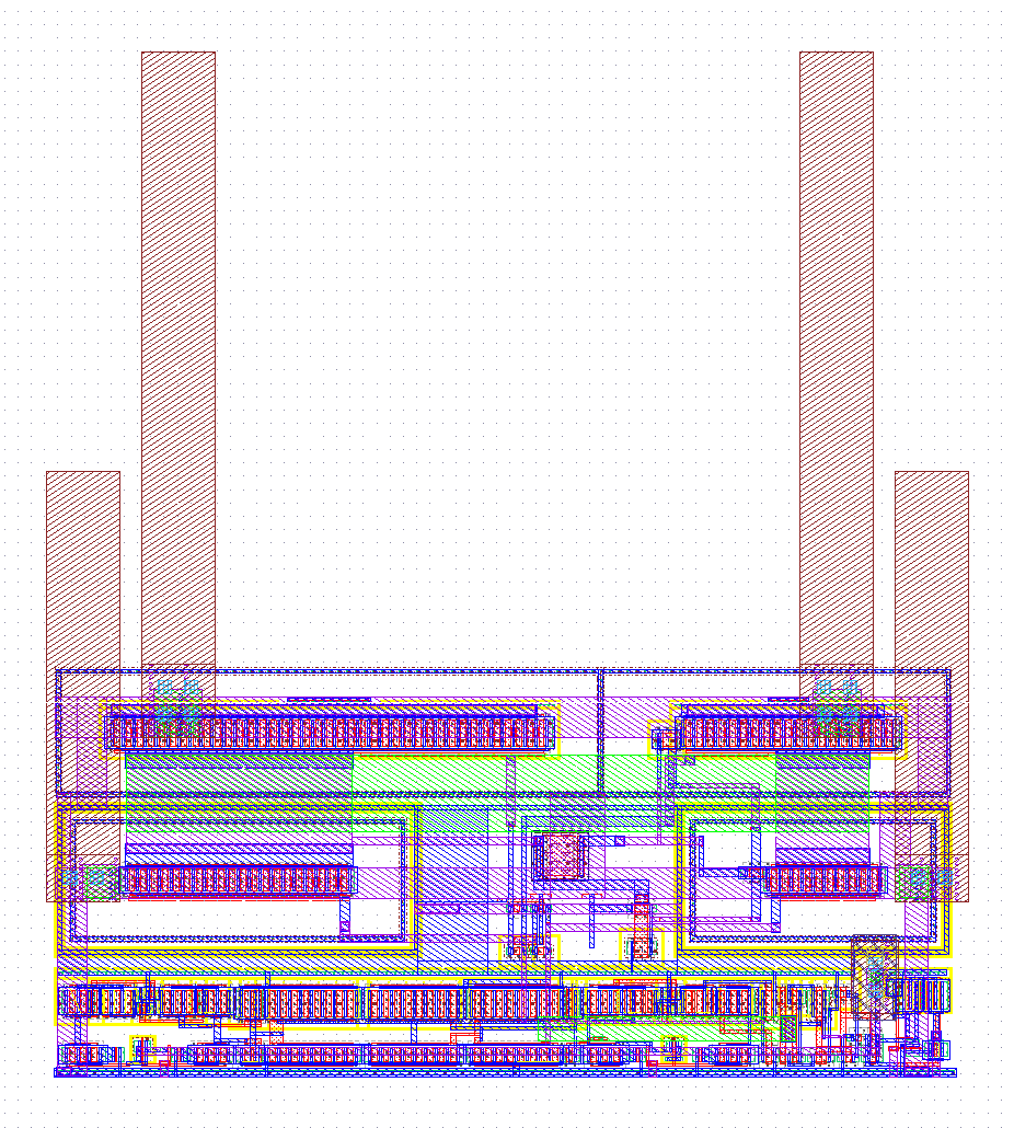
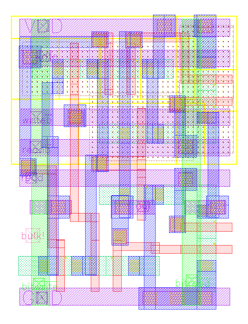
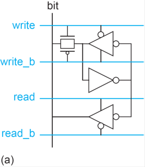
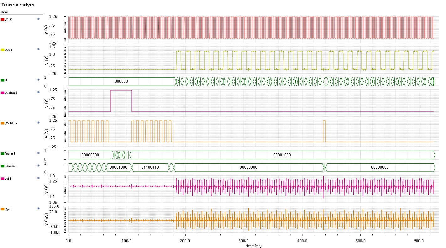
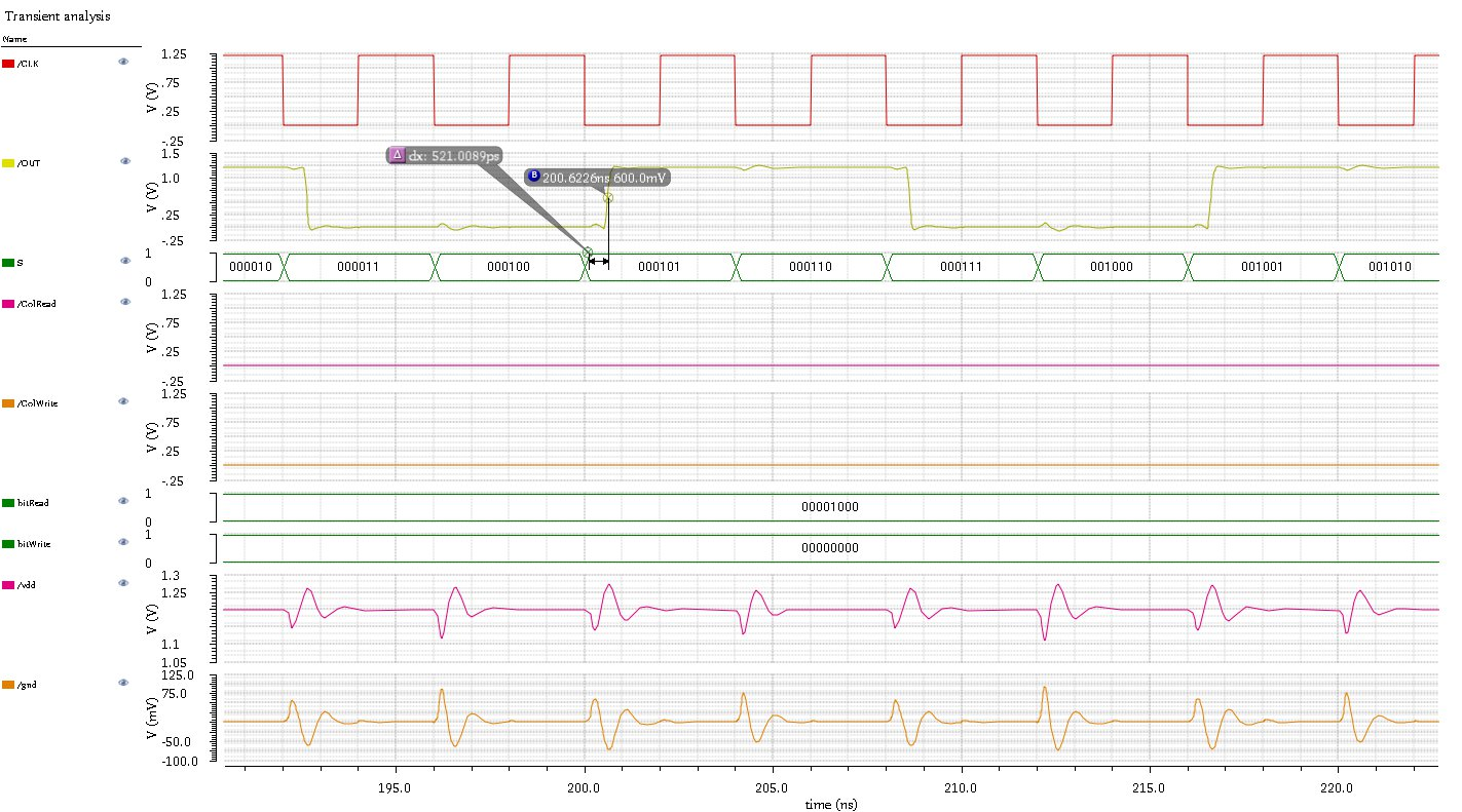
12T SRAM cell
We chose to use 12 transistors to implement our SRAM cell as the design offers great reliability of reading and writing into the SRAM. In addition, 12T SRAM design does not need bitline to be precharged, indeed such a design does not need a clock. So 12T SRAM offers much greater probability of having a functioning chip. As a trade-off, 12T SRAM requires a larger area compared to traditional 6T SRAM design. However, we are able to push the limit and have a compact 12T layout that appears smaller than the 12T SRAM design layout in CMOS VLSI Design by Neil Weste and David Harris [8].
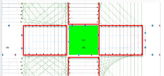
CLB
CLB consists of 6 stages of MUX tree that forms a lookup table. One CLB will take 6 bits of input and produce 1 bit output from its lookup table. On top of that, CLB can be programmed to have asynchronous output with 500ps delay.
ISB
The internal switch block is based on Wilton switch block topology. It has the highest routability among all three most common switch blocks in FPGA design with the expense of area [5]. The switches are implemented using transmission gates [6].
Horizontal and Vertical Connection Blocks
The connection block serves as an inferface between CLBs and the routing grid, and contains buffers and tristate drivers.
Clock architecture
In our FPGA design, a combination of H-tree and grid clock architectures were implemented. In addition, ground shields between clock H-tree and surrounding clock grid were placed. Benefiting from such clock circuitry implementation, a rise and fall time of 300ps is achieved. The delay from H-tree input to internal clock grid is 1.2ns. The simulated performance data suggests that core max clock frequency is 250MHz.