
System Modeling
Bitstream Generation
Despite all that VTR does, the tool only comprises a small fraction of the software needed to synthesize programs onto our FPGA. VTR only generates files with information about what each LUT contains and which routing tracks are active, but no information about how to configure and interface with a physical FPGA.
The first step is to translate the outputs of the VTR flow (.blif, .net, .place, & .route files) into the 1's and 0's that must be loaded into each SRAM cell. To do this, we wrote a Scala wrapper that parses the VTR outputs with knowledge of the general FPGA architecture into a bitstream. This bitstream then gets hard-coded into the assembly of the Chisel HDL model or loaded into the FPGA in the structural simulations. These two processes are described below.
HDL Model & Validation
To validate the behavior of the architecture for a given bitstream, we must generate an HDL definition of our FPGA. Continuing the spirit of using open-source tools, we used the Chisel HDL, developed at UC Berkeley. Embedded in the Scala programming language, it is a new, hierarchical and object-oriented alternative to existing HDLs such as VHDL and Verilog.
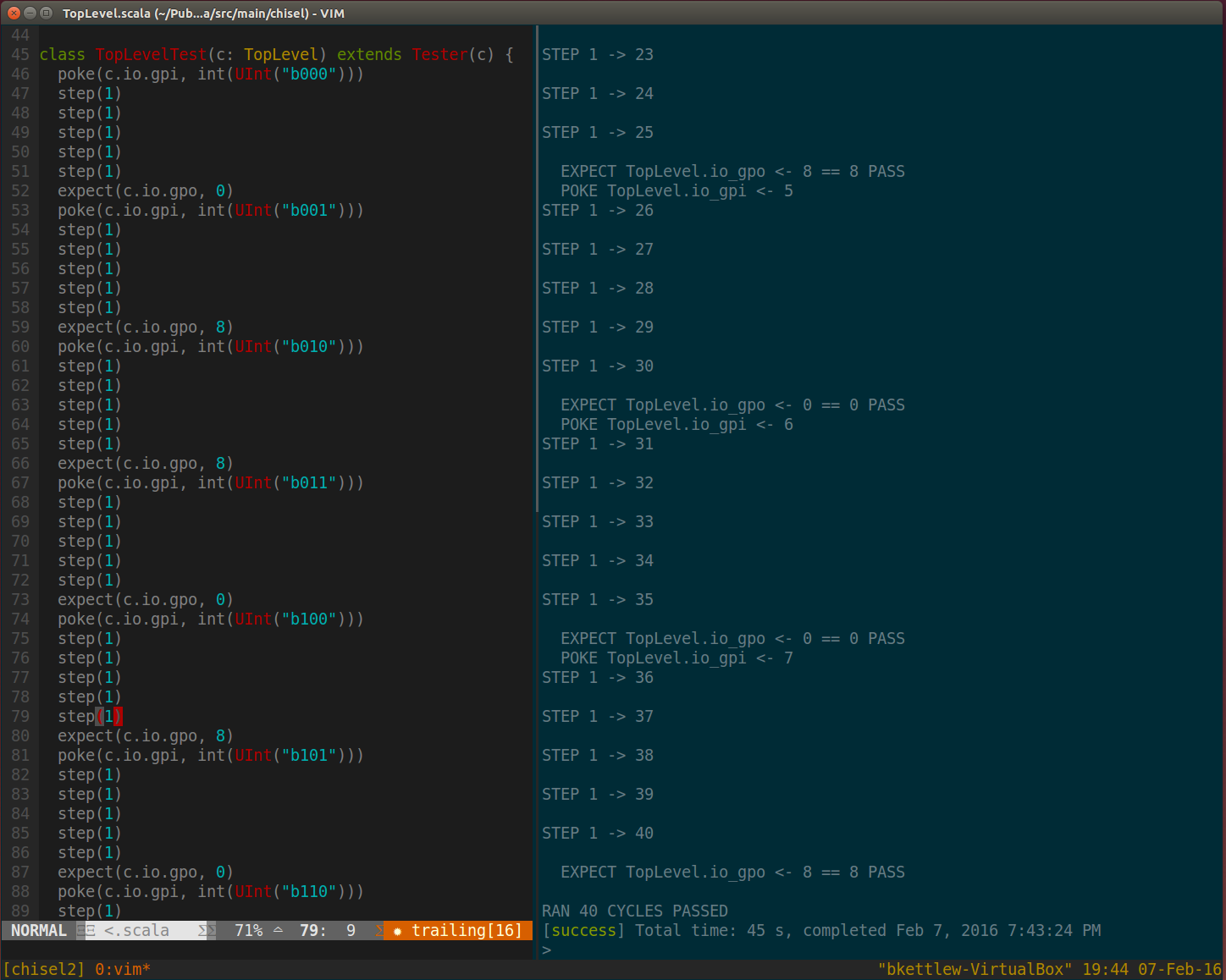
All the internal and external functionality and connectivity as described in the Architecture page is written in Chisel to create a comprehensive behavioral model of the FPGA. Great care was taken to make the model scalable so that changes to the size of the FPGA driven by the IC design process can be quickly back-annotated into the model. The only major challenges we encountered when using Chisel were the lack of tri-state logic and the presence of infinite combinational loops. The lack of tri-state logic drove transistor-level design that eliminated floating nets, while the combinational loops problem would never actually happen after synthesizing programs using the VTR flow.
Finally, we assemble our FPGA with the bitstream given by the Scala wrapper above. Using Chisel "pokes" and "peeks", we can test the behavior of the fully-assembled Chisel model:
Structural Simulations
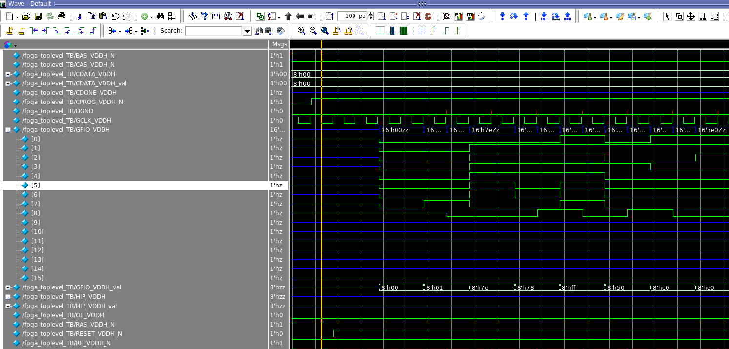
After completing the transistor-level design of the FPGA, we exported the design as a Verilog structural model. Some workarounds were necessary to effectively model the SRAM cells and the tri-state transmission gates. We wrote a comprehensive Modelsim testbench that emulated the behavior of a microcontroller in configuring the FPGA with a bitstream, and then verified the FPGA's response to stimuli on the GPIO and HIP pins for various arithmetic functions. Modelsim helped us find and correct a few connectivity errors. An example simulation is shown below:

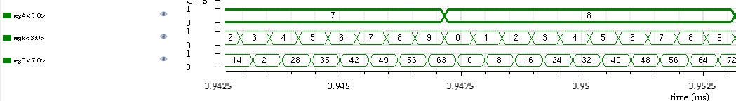
To better understand the true performance of the FPGA, we also exported the transistor-level design to SPICE netlists in order to script Ultrasim simulations. Numerous workarounds had to be made in order to integrate the ARM standard-cell decoders with the custom-designed blocks. Additionally, the design was so complex that only the fastest digital optimizations in Ultrasim could yield simulations that only took a few hours on the lab computers. In the end, the Ultrasim simulations also validated the behavior demonstrated in the behavioral Chisel and structural Modelsim simulations:
All of the tools and code used in modeling and validation of the FPGA can be found in the trollstigen-fpga Github repository.