
Demoboard PCB Design Overview
Our PCB design for the demoboard shown below consisted of a 4 layer stackup with trace widths selected for a 50 ohm routing impedance. We used Circuit Maker as our EDA tool since we were able to collaborate remotely on the routing and work in parallel which greatly improved our efficiency. The demoboard was designed to have the proper form factor to act as a "hat" for the Raspberry Pi 3.
Schematic Design
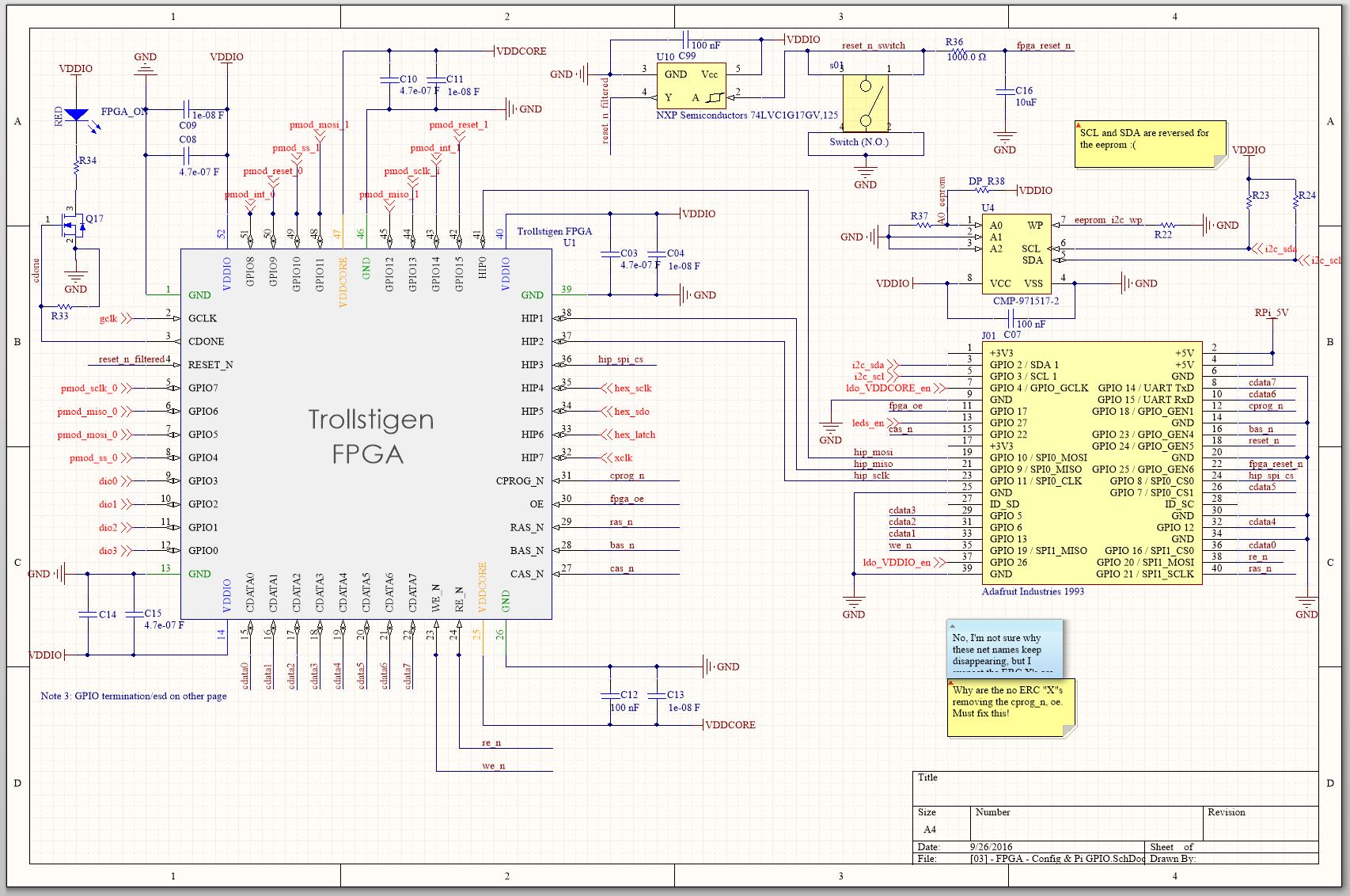
Fig. 1 - Main FPGA schematic page
PCB Design
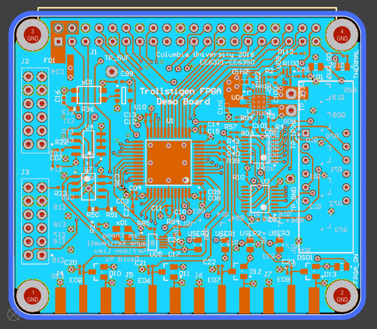
Fig. 1 - Component side of PCB
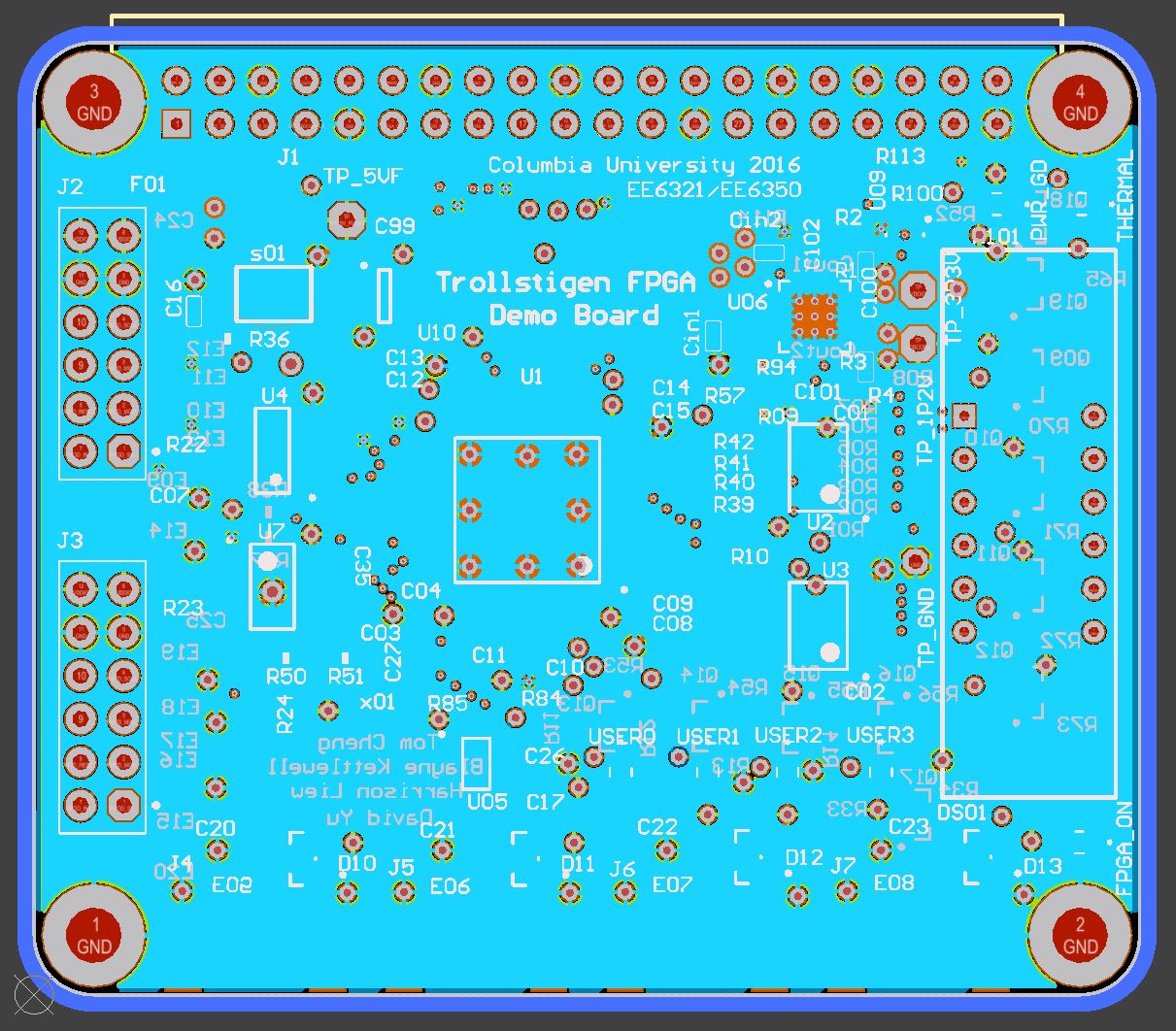
Fig. 2 - Ground layer of PCB
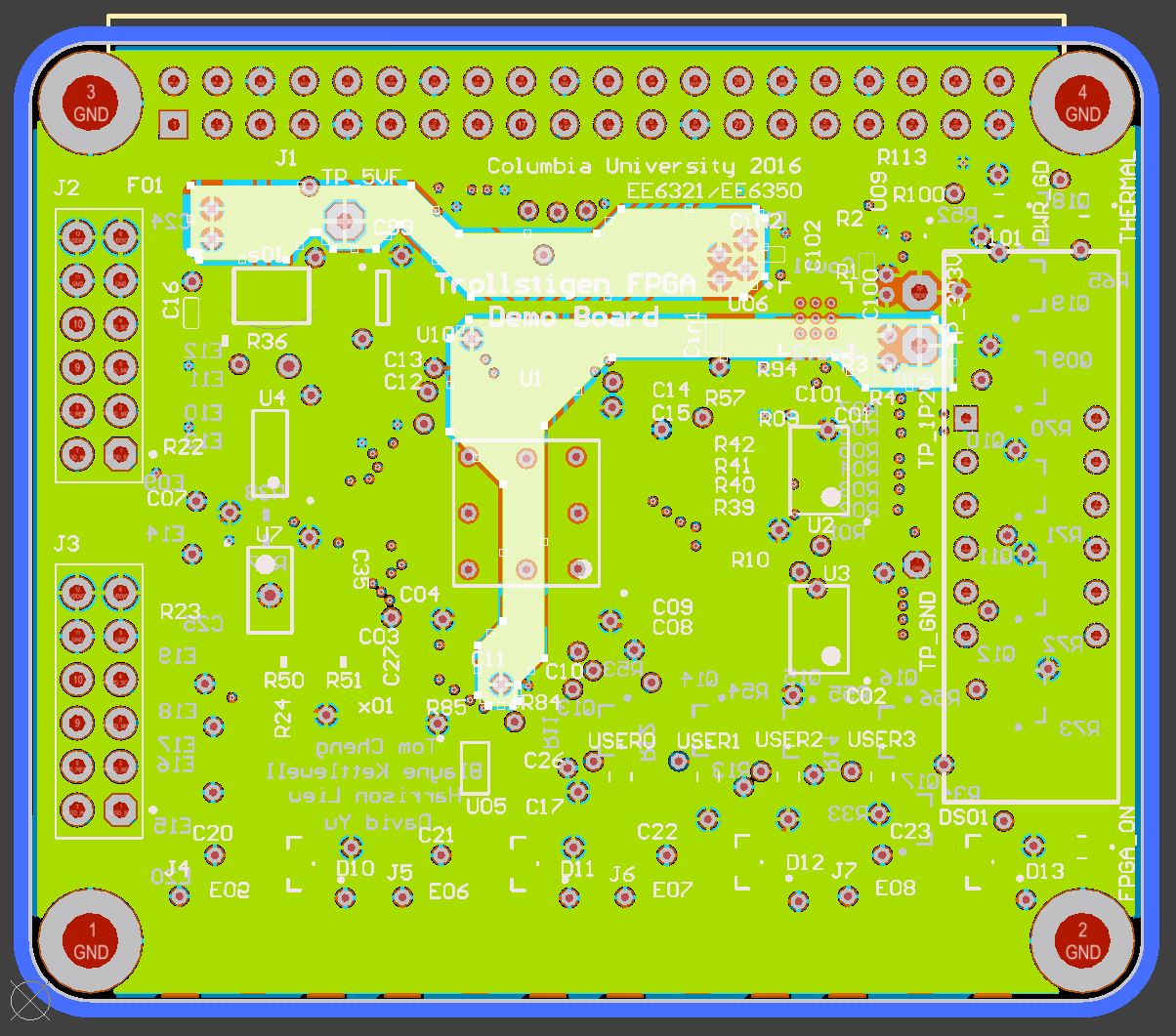
Fig. 3 - Power layer of PCB. Note, the two internal power planes for 1.2V and 5V are highlighted, everything else is 3.3V.
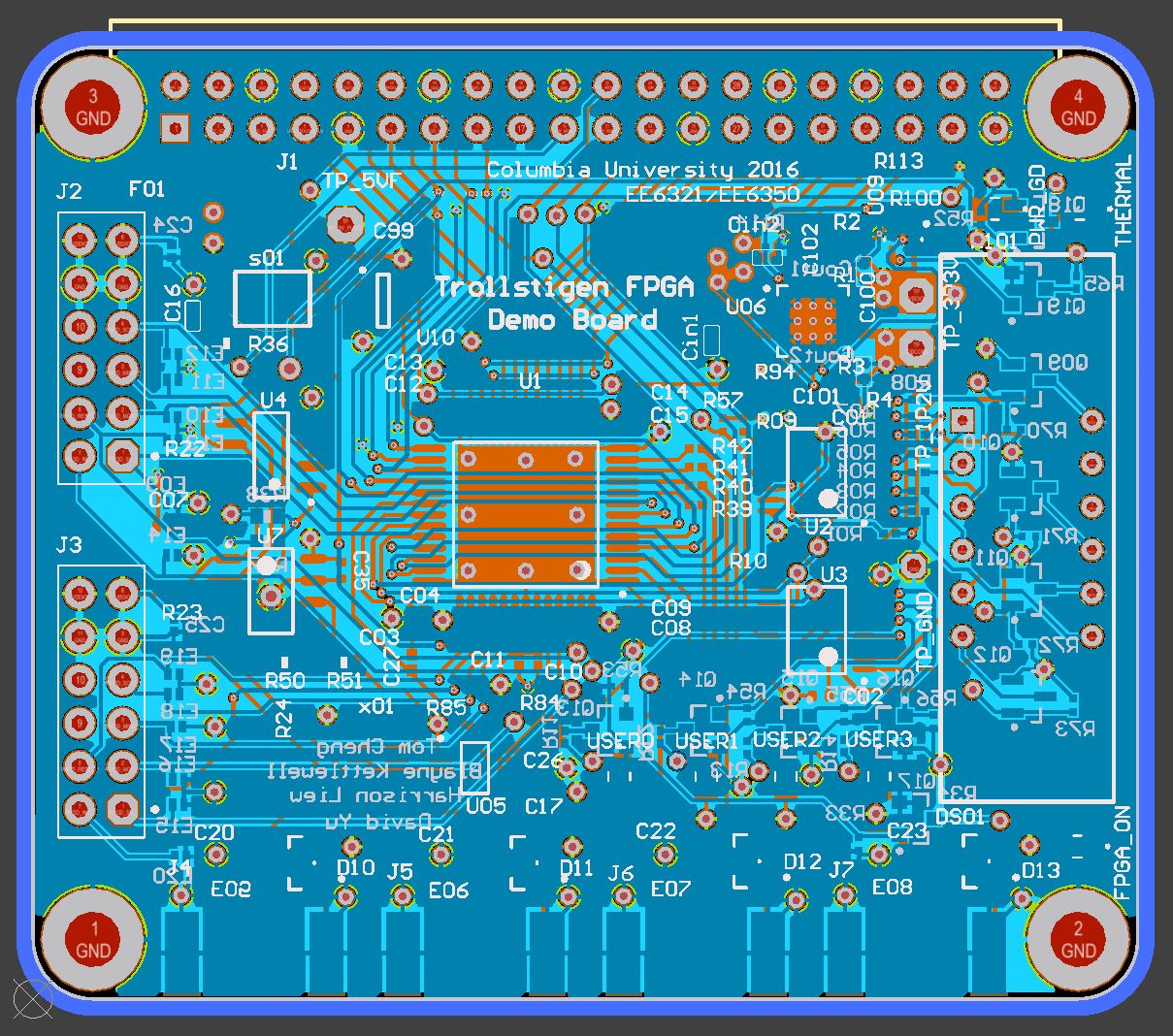
Fig. 4 - Solder side of PCB
Assembled Demoboard
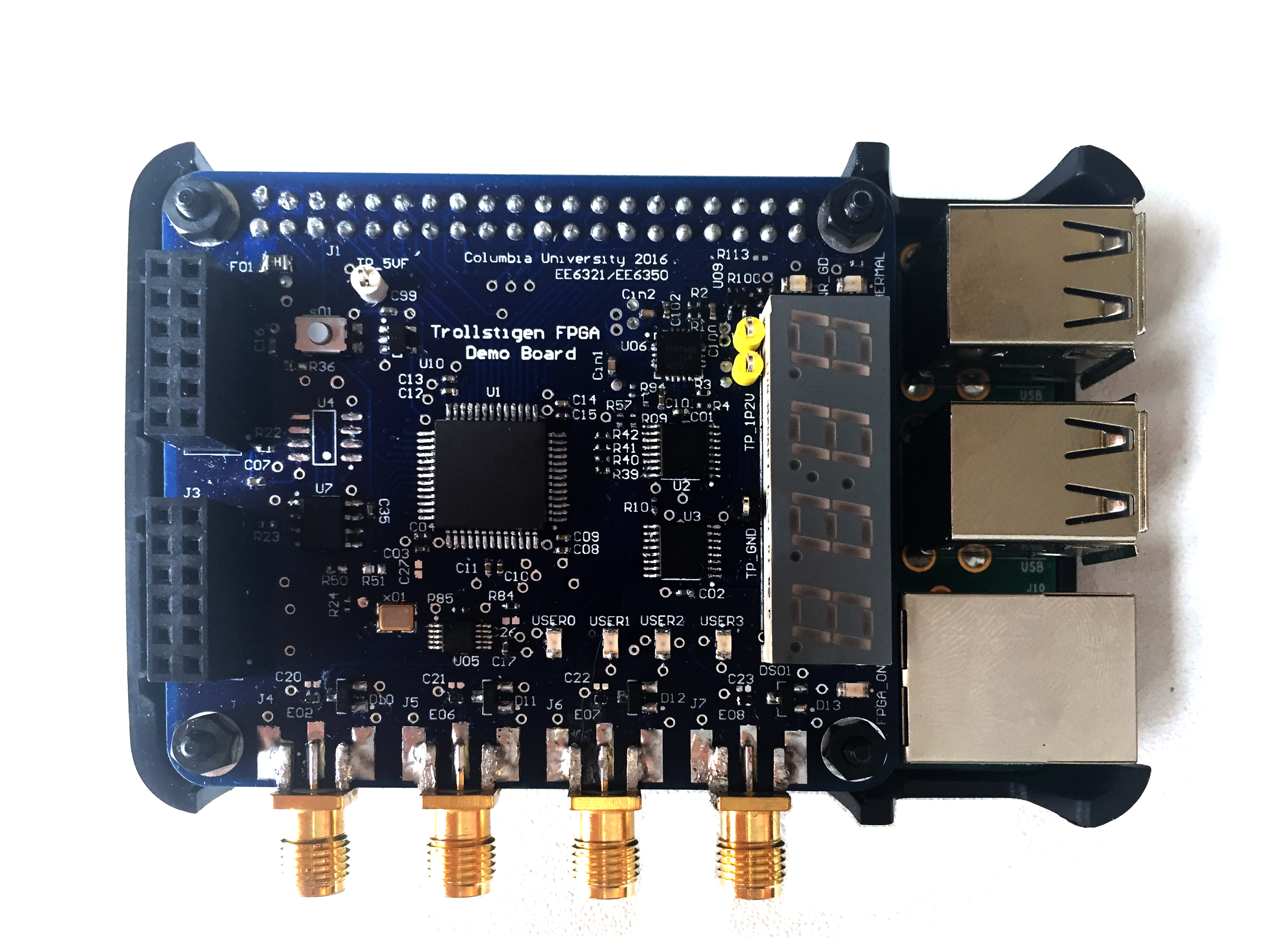
Fig. 5 - The final assembled demoboard "hat" mated to the Raspberry Pi 3