Architecture
Introduction to FPGAs
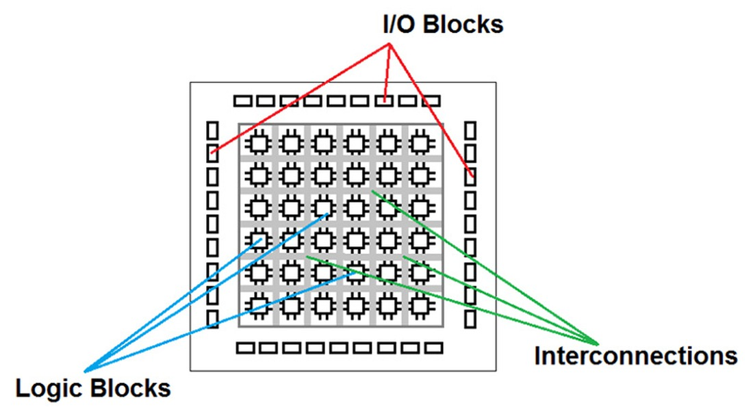
A Field Programmable Gate Array (FPGA) is a computing architecture comprised of a fabric of configurable logic resources. Its main advantage over other computer architectures is that they can be reconfigured to solve any problem computable by a processor or ASIC, while offering a significant performance advantage for highly parallelized or timing-sensitive applications. It has already found its way into products ranging from medical imaging to high-performance communications processing, and are beginning to appear in full SoCs as soft, reconfigurable processor cores and hardware accelerators. At a high level, the internal structure of an FPGA looks like this:
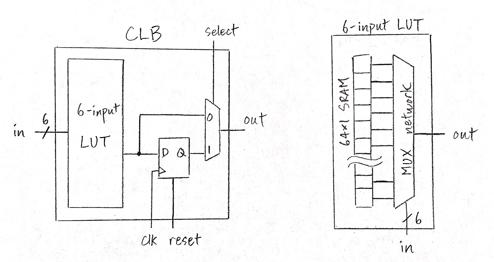
As shown above, the logic power of the FPGA is contained in configurable logic blocks (CLBs). In our implementation, each CLB is a 6-input look-up table (LUT). This means that 6 separate input bits to the CLB select one out of the 64 bits in the LUT for the output. Every bit in the LUT is stored in a 12-T SRAM cell. An additional D Flip-Flop allows for the choice of synchronous or combinational logic.
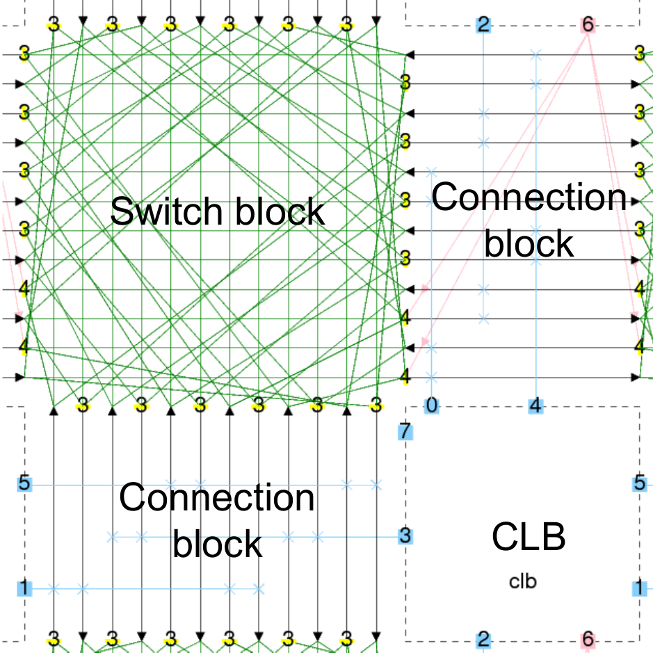
In order to complete the fabric, signals must be routed between each CLB. On each edge of a CLB, we have Connection Blocks that connect the horizontal and vertical routing tracks to the inputs and output of the CLB. At the intersections of these routing tracks, a Switch Block allows signals coming in from one direction to turn towards any of the remaining three directions. The Wilton switch block topology was chosen, which allows for high routability at the expense of some area. With the limited number of CLBs we could fit on our die, this was the best topology to ensure that we could use 100% of our logic resources for any given application. Every stage of the interconnect is turned on or off using a transmission gate controlled by an SRAM. Below is a conceptual diagram of how the various blocks are connected together into a "tile" structure that can be replicated almost infinitely in both dimensions. The possible connections in the switch blocks are shown by the green lines.
Core Architecture Definition
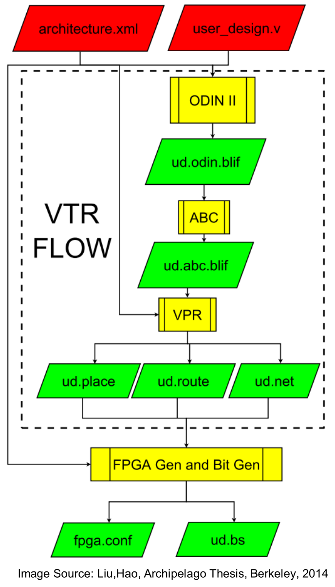
To develop an architecture for our FPGA core, we used the Open Source Verilog to Routing tool, the product of a worldwide collaborative effort to provide an open-source framework for conducting research and development on FPGA development and CAD. The VTR design flow takes as inputs a Verilog description of a digital circuit and the target FPGA architecture. It then performs:
- Elaboration & Synthesis using ODIN II
- Logic Optimization & Technology using ABC
- Packing, Placement, Routing, & Timing Analysis using VPR
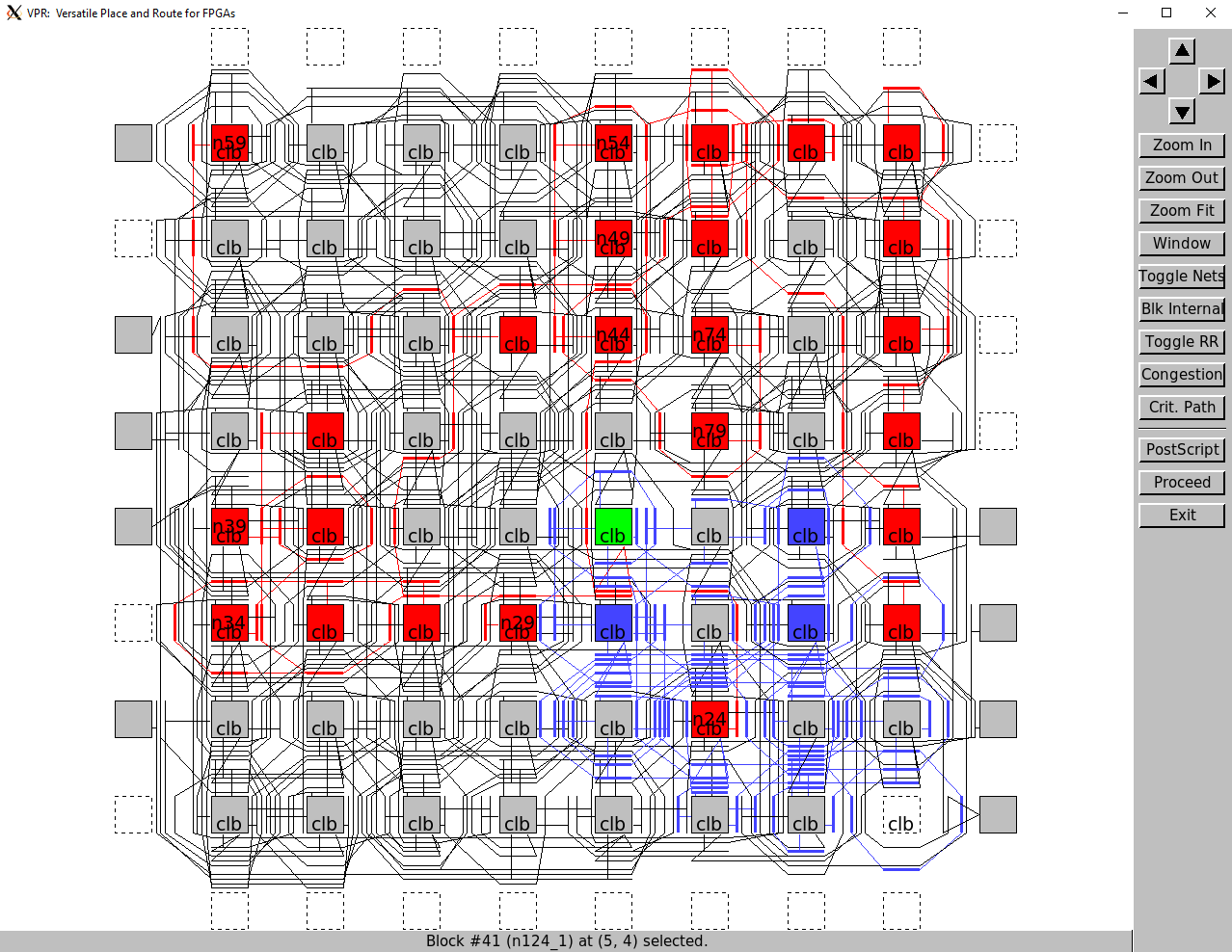
As the IC design process advanced, area and pin constraints drove constant adjustments in our architecture. With VTR, we were able to quickly redefine our FPGA architecture, then validate it as will be described in the next section, System Modeling. In the end, we were able to settle on an 8x8 CLB structure as shown in the VPR GUI:
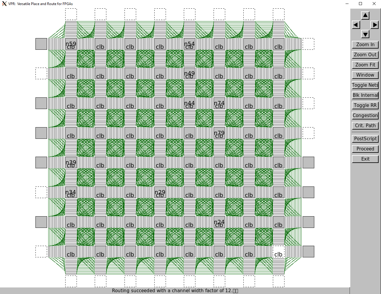
VTR reliably synthesizes Verilog programs (digital circuits) onto our FPGA, and shows the resource utilization of the program. An example program (Digital Thermometer demonstration) is shown below. VPR allows you to visually understand and validate the logic synthesis. The active I/O pads & CLBs are the grey boxes and the active interconnects are the black lines. To examine the inputs and outputs to a given CLB by clicking on it. For example, the outputs of the CLBs highlighted in blue are routed to the inputs to the selected CLB highlighted in green. In turn, the output of the selected green CLB fans out to all the CLBs highlighted in red.
Top-Level Interface Definition
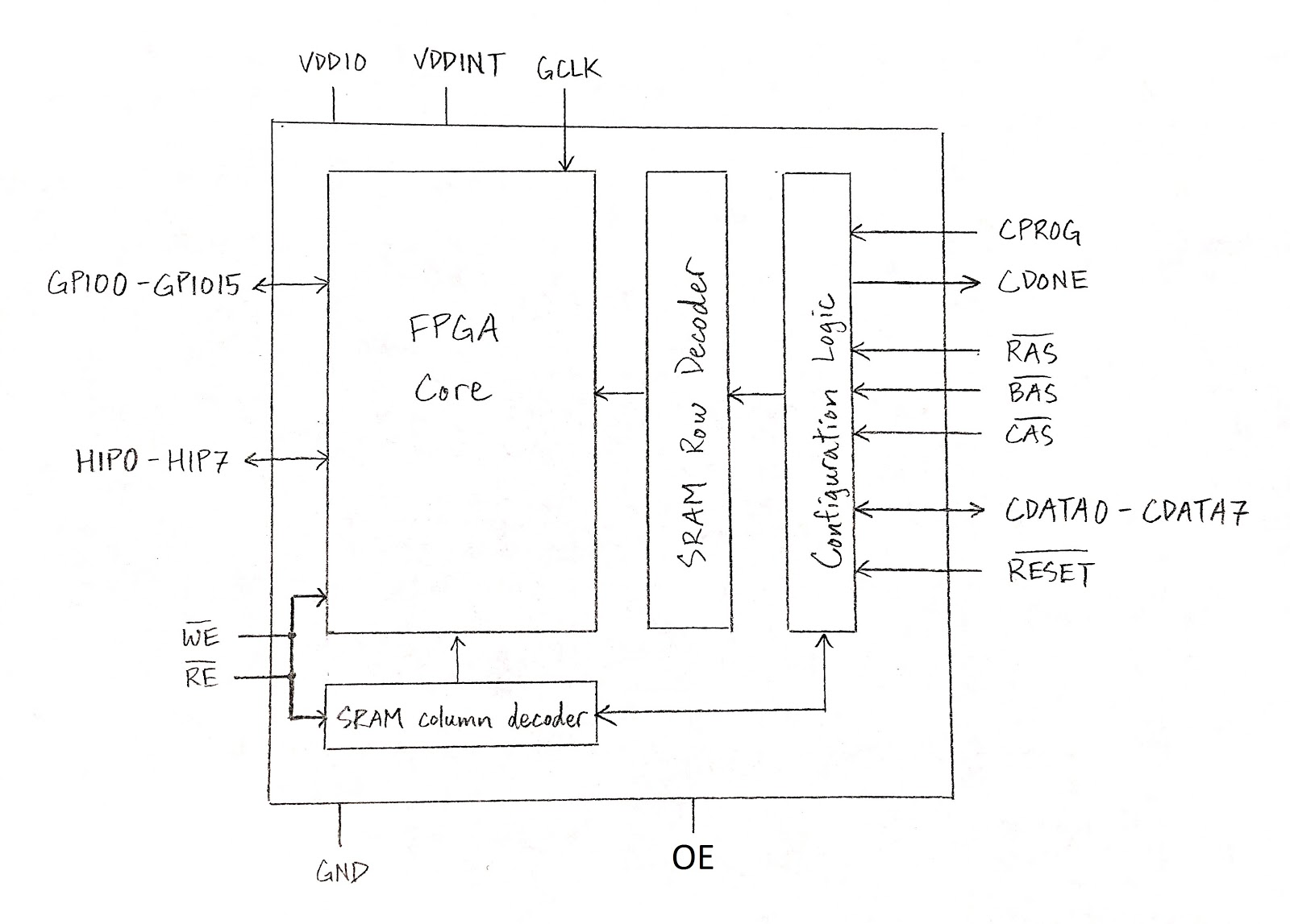
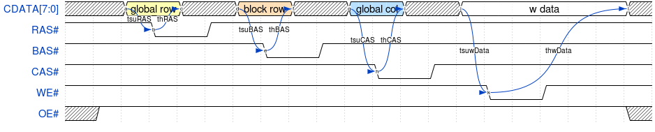
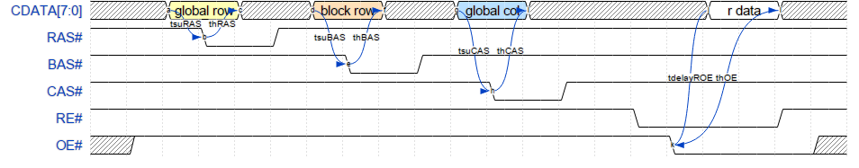
Recall that all the LUT values and the interconnect controls in the FPGA core are stored in SRAM cells. To load the correct configuration values into all the SRAM cells, we defined an asynchronous, parallel configuration bus. Operating similarly to DRAM, it has 8 bits of parallel data along with row/column decoders so that we can select a byte of SRAM at any given row and column and then write the configuration data. Our design also allowed for configuration readback, so that we can detect any non-functional SRAM cells. Finally, with the 52-pin package afforded to us, we were able to fit 16 GPIO ports and 8 Host Interface Ports (HIP). The final top-level diagram and configuration/readback diagrams are shown below.