
Board-Level Testing and Functional Validation
Our post tape-out testing methodology was broken into two phases: the first of which was board-level testing and the second functional testing. The board-level testing was used in order to validate that the Raspberry Pi 3 would properly enable the power supplies and be able to steer the programmable clock generator to our frequencies of interest. Furthermore, we wanted to validate that our PCB design had acceptable signal integrity characteristics which would be sufficient for the needs of our project.
Prior to receiving our custom FPGA from MOSIS, we used a Xilinx FPGA to mimic our custom asynchronous programming interface, so we could test our host level bitstream download/configuration code. This greatly improved the bring-up process since we had strong confidence that, if our chip was defect free from fabrication, it would work immediately. This proved to be the case, since our initial SRAM write and read back testing benchmarks worked within minutes of soldering our FPGA to our first produced demoboard.
Since our chip design was largely digital and we were pin limited with our 52 pin QFP package, we decided not to break out any internal nets to characterize the process corner of our chips.
Board-Level Testing
Power Supplies:
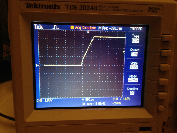
Fig. 1 - LDO Output: Power Enabled, Ramp-up 3.3V
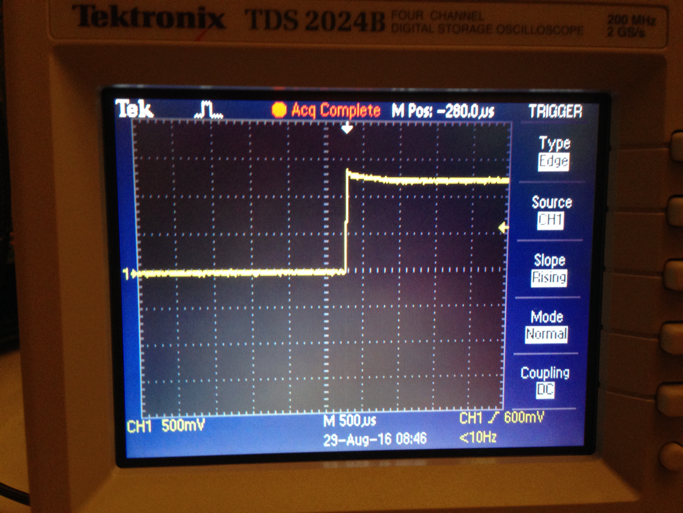
Fig. 2 - LDO Output: Power Enabled, Ramp-up 1.2V
Clocks:
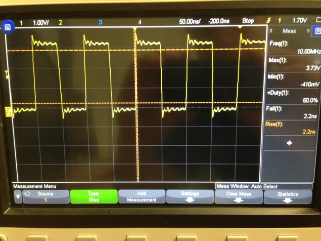
Fig. 3 - Si5351 Clock generator CLK_0 output. [Top-level clock] "GCLK", programmed to be 10MHz.
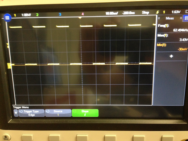
Fig. 4 - Si5351 Clock generator CLK_1 output. [Sample clock] "XCLK", programmed to be 62.5KHz.
FPGA Reset:
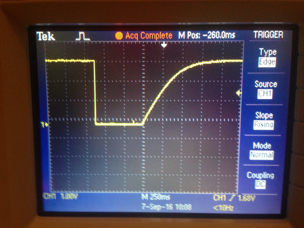
Fig. 5 - FPGA Reset, Pre-Schmitt trigger. Note the large RC time for deactivating the reset. This is due to the weak ~51K ohm internal pull up from the Raspberry Pi3 which is connected to this line and our desire to try to minimize the bounce upon releasing the reset switch.
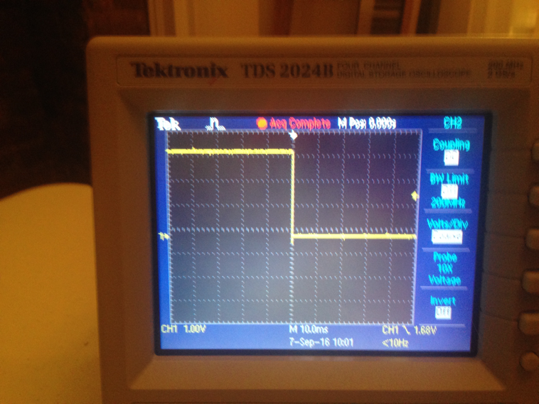
Fig. 6 - FPGA Reset, Post-Schmitt trigger, falling edge.
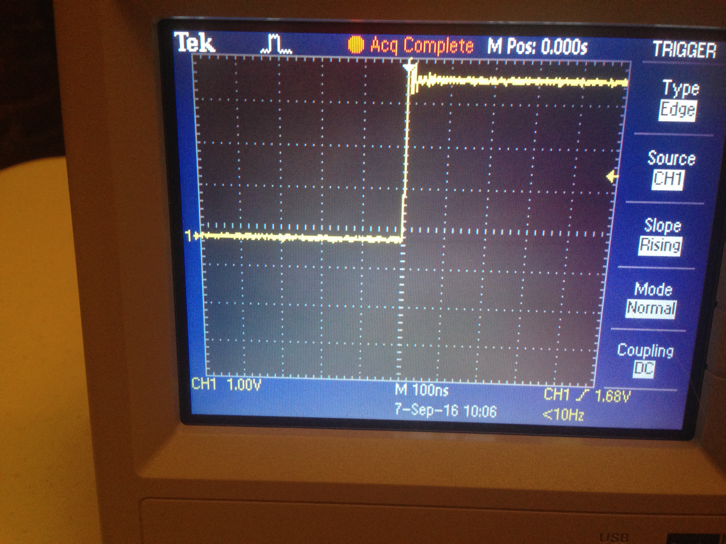
Fig. 7 - FPGA Reset, Post-Schmitt trigger, rising edge.
7 Segment Display
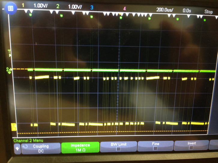
Fig. 8 - HEX_SDO (Yellow) and HEX_LATCH(Green) signals from the FPGA measured at the input pins of the external serial latch.
General Purpose I/O:
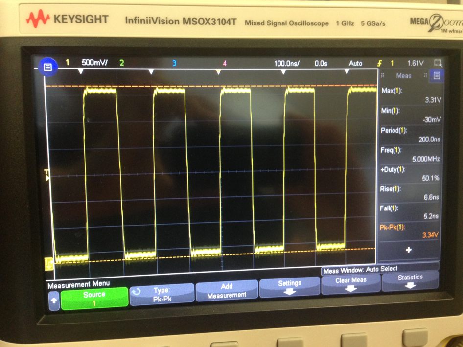
Fig. 9 - GPIO0 from the FPGA measured at the SMA side mounted connector. This signal was generated from the Counter demo with the "Top-Level" GCLK running at 10MHz. The rising and falling edges of this signal are clean and there is negligible overshoot or undershoot.
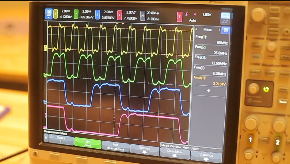
Fig. 10 Counter application running with a GCLK of 100MHz on the FPGA with the 4-bit result being mapped to GPIO0-3. The SMA connectors were connected to the scope via SMA to BNC cables (50 ohm). One can see a slight reflection in the waveforms since the output impedance of our bidirectional level translator circuits was higher than the 50 ohm transmission line, so there was no way to minimize the reflection through series termination resistor selection.
Functional Validation
Given that our design was digitally oriented, our benchmark for success was demonstrating that our custom FPGA could correctly run arbitrary applications that were written in Verilog and synthesized, placed and routed using the VTR tool. Our more specific goal was to meet timing at a Top-Level clock rate of at least 10MHz. In the end, we were able to run all of the applications outlined below in excess of 30MHz, with the 4-Bit Counter running at 100MHz. All of these applications exhibited correct functional behavior.
- 4-Bit Counter (Figure. 10 above)
- Stopwatch
- Digital Thermometer
- Gene Sequencing (See video for demonstration)
- Encryption (See video for demonstration)
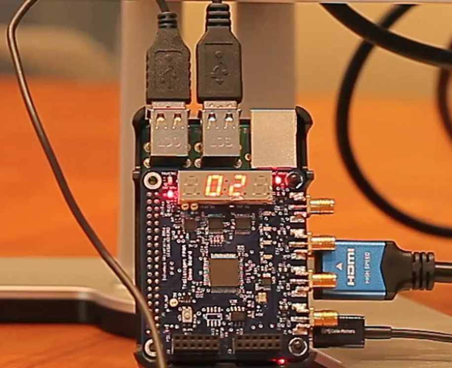
Fig. 11 - Stopwatch demo showing the seven segment display incrementing from 0 through 15. This display is updated through a simplified SPI master protocol coming from our FPGA.
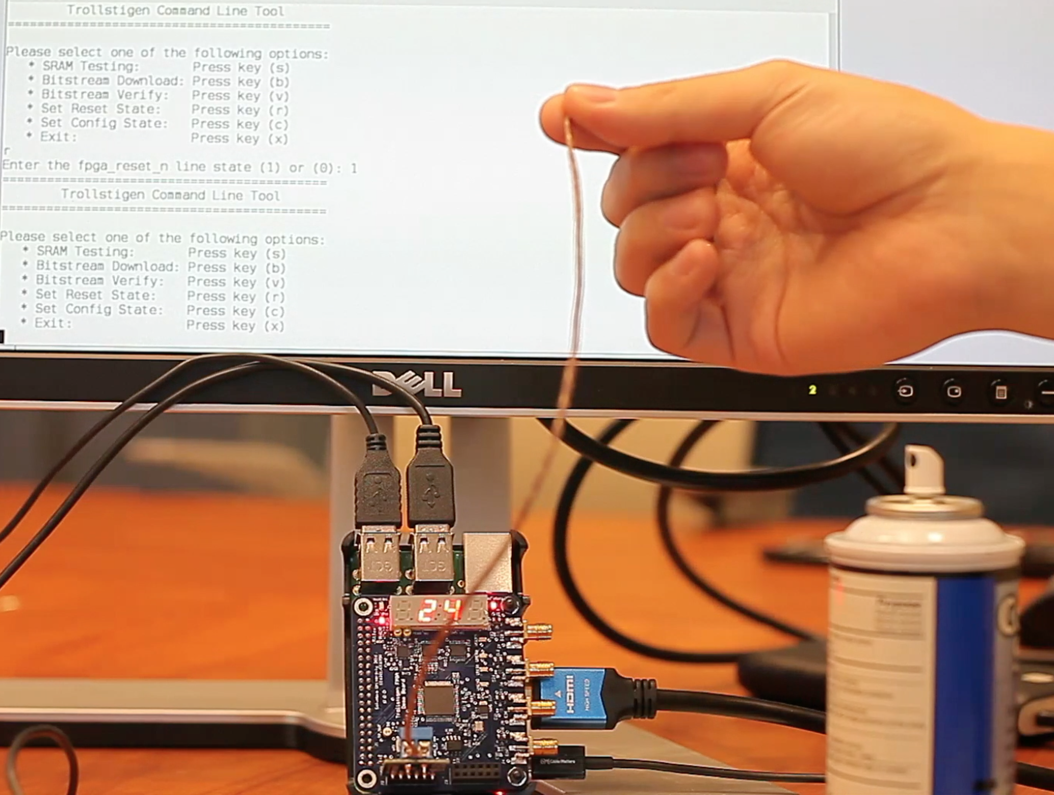
Fig. 12 Digital Thermometer which obtains digitally converted temperature readings from a SPI based thermocouple Pmod sensor. This data is then converted from base 2 to degrees centigrade in the FPGA via a look-up table (LUT) mapping. These converted values are then serially fed to the two digits of the seven segment display.
Given that our design was digitally oriented, our benchmark for success was demonstrating that our custom FPGA could correctly run arbitrary applications that were written in Verilog and synthesized, placed and routed using the VTR tool. Our more specific goal was to meet timing at a Top-Level clock rate of at least 10MHz. In the end, we were able to run all of the applications outlined below in excess of 30MHz, with the 4-Bit Counter running at 100MHz. All of these applications exhibited correct functional behavior.
- 4-Bit Counter (Figure. 10 above)
- Stopwatch
- Digital Thermometer
- Gene Sequencing (See video for demonstration)
- Encryption (See video for demonstration)
Fig. 11 - Stopwatch demo showing the seven segment display incrementing from 0 through 15. This display is updated through a simplified SPI master protocol coming from our FPGA.
Fig. 12 Digital Thermometer which obtains digitally converted temperature readings from a SPI based thermocouple Pmod sensor. This data is then converted from base 2 to degrees centigrade in the FPGA via a look-up table (LUT) mapping. These converted values are then serially fed to the two digits of the seven segment display.