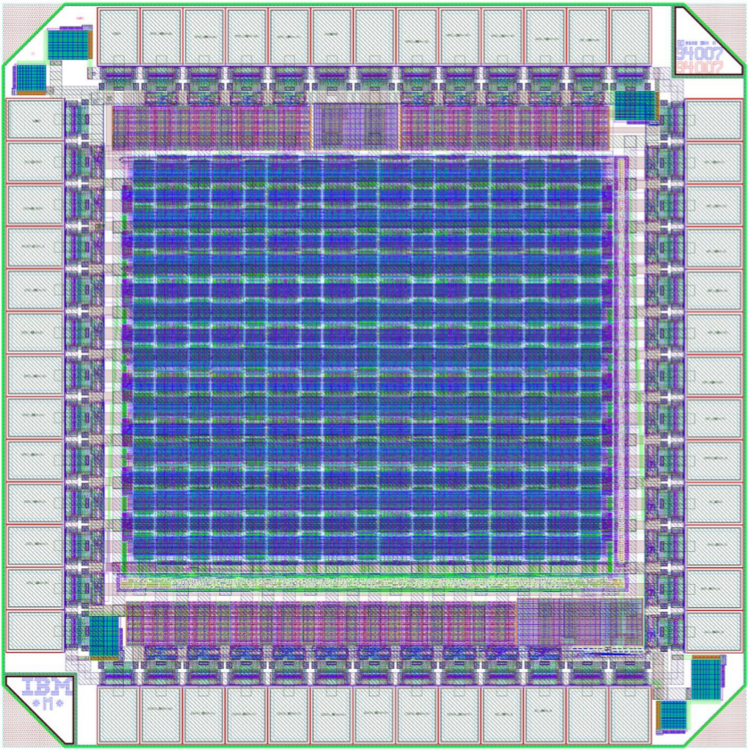
IC Layout
IC design was done in custom and digital flow using Cadence Virtuoso, Verilog, Synopsys Design Compiler, ARM standard cell library, Modelsim, licensed to Columbia University. The chip is fabricated using 130nm IBM technology on 2.25mm2 silicon. The FPGA used 52-pin QFP open cavity wirebond package.
Macro Blocks
The FPGA's core consists 64 tiles, and 4 macro blocks form one tile. The 4 macro blocks are CLB (configurable logic block), ISB (internal switch block), HCB (horizontal connection block), and VCB (vertical connection block).
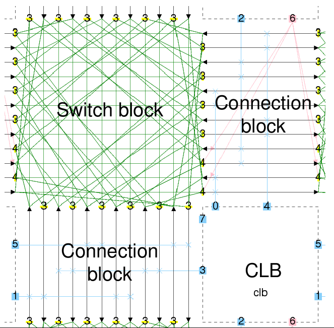
CLB
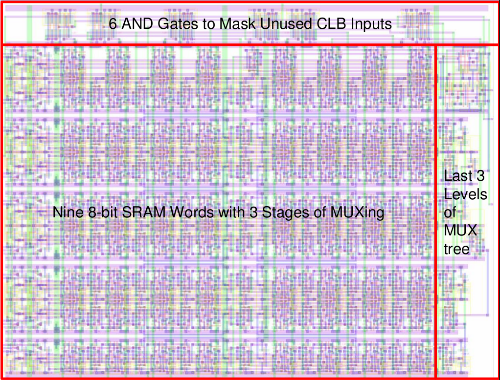
The CLB contains 6-input LUT (64 bits) with 6-stage MUX tree. In addtion, D flip-flop and final 2:1 MUX allows a choice between asynchronous and synchronous outputs.
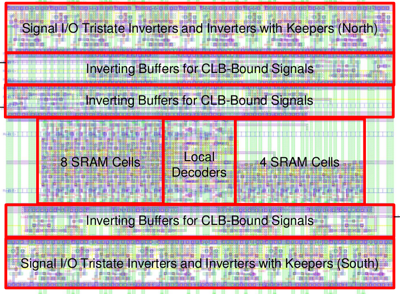
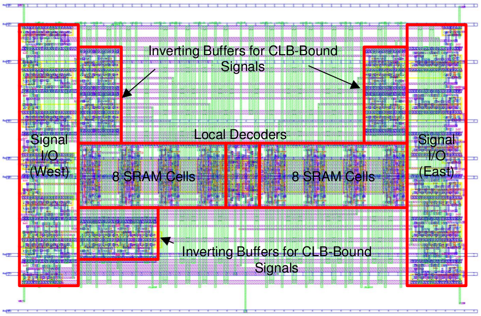
ISB
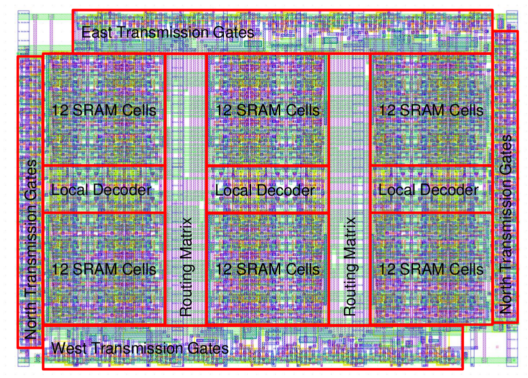
The ISB contains 72 SRAM cells arranged in quadrants and the connectivity can be programmed through writing to the SRAMs.
HCB & VCB
HCB and VCB interface between CLBs and the routing grid, and contains routing buffers and tristate drivers.