
System Architecture
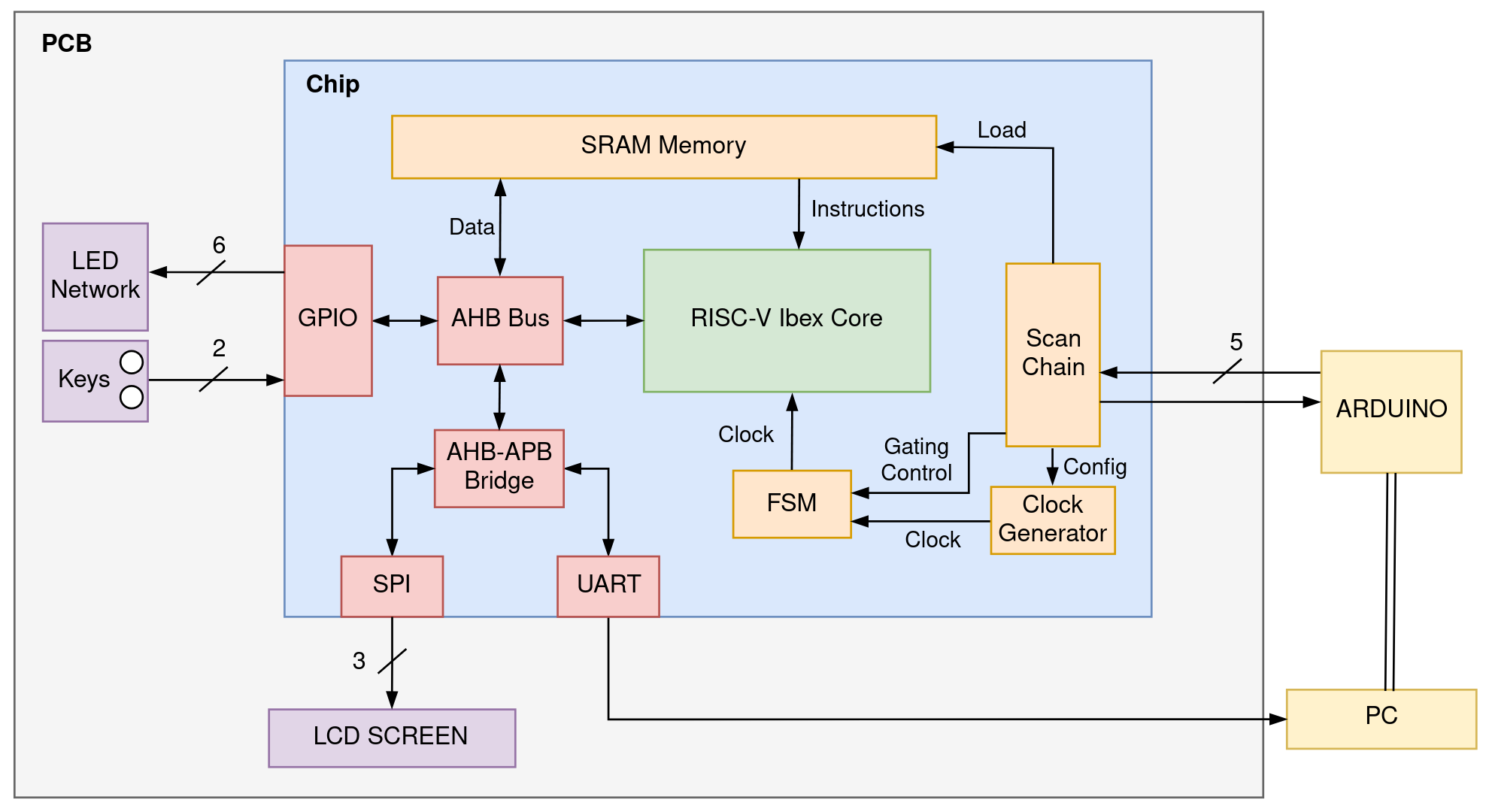
Figure 2 displays a high-level block diagram of the proposed system, which provides an insight into the building blocks and interface of the chip. As shown, the RISC-V CPU is the heart of the design and is surrounded by multiple components that enable it to communicate with the outside world and demonstrate its capabilities. This section is dedicated in describing the importance and details of every component of the chip.
RISC-V CPU
For this project, the open source 32-bit Ibex RISC-V CPU core [1], currently maintained by lowRISC, was deployed. This core has been heavily verified, has seen multiple tape-outs and provides a well defined software support, features that made it ideal for the purposes of this project, as it removes the high development effort required to build a CPU from scratch and minimizes the risk of introducting functional bugs during RTL design.
From the multiple core configurations offered by lowRISC, the "small" version was adopted. This core supports the RV32IMC instruction set, that is it supports the Integer Multiplication and Division Instructions and the Compressed Instructions extensions. It has a 2-stage pipeline (Instruction Fetch & Instruction Decode/Execute) and it comes with a 3-cycle multiplier. Although other available features such as a Branch Predictor or a Writeback stage would not affect our design workload, we avoided adding them in the core to keep the overall design as simple and small as possible, since this project did not aim to achieve high performance. A high level overview of the core's basic components is given in Figure 3.
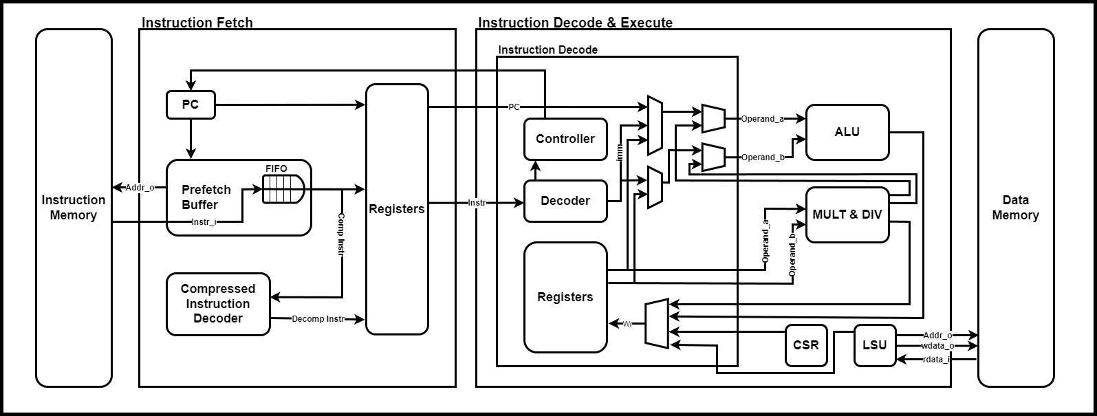
As described in the Ibex Reference Guide [2], the core is capable of fetching 1 instruction per cycle via a prefetch buffer. Multicycle instructions, such as multiplication or memory accessing, stall the ID/EX stage until they complete. The core has an Instruction Memory Interface to fetch instructions from the on-chip memory. Similarly the Load-Store Unit (LSU) is responsible for transferring data from and to the memory. Generally, the processor supports trap handling for interrupts and exceptions through its Control and Status Registers (CSRs), but this functionality has not been used or tested in this project.
Memory
One of the most important parts of processor design is the amount of memory that can be integrated on chip. Our chip features 64KB of on-chip SRAM memory, evenly divided for instructions and data. More specifically, the ARM Artisan Memory Compiler was used to generate two 1-port 32KB memory modules, one used as Instruction Memory and one for Data Memory. Although the memory compilation process was quite straightforward, wrappers were designed around the memory modules to enable their integration with the core, given the core's interface, as well as data/instruction loading during system initialization through a scan chain.
Control & Debugging Blocks
The three blocks colored orange at the right side of the chip diagram (Scan Chain, Clock Generator and FSM) are essential for the correct operation of the chip, as they are responsible for initialization, control and debugging.
Scan Chain
The Scan Chain provides the user with the only access point to the on-chip memory and enables data loading and reading. In particular, the scan chain is connected to the memory modules and is used to load a program's instructions and data before turning on the processor. As explained in later sections, it is also connected to the Clock Generator and FSM modules to load the appropriate values to their configuration registers during setup. Moreover, for debugging purposes it can be used to read out data from the data memory to verify that the processor operates correctly, e.g. reading out the stored result of an arithmetic operation. A simplified diagram of the scan chain is given in Figure 4.
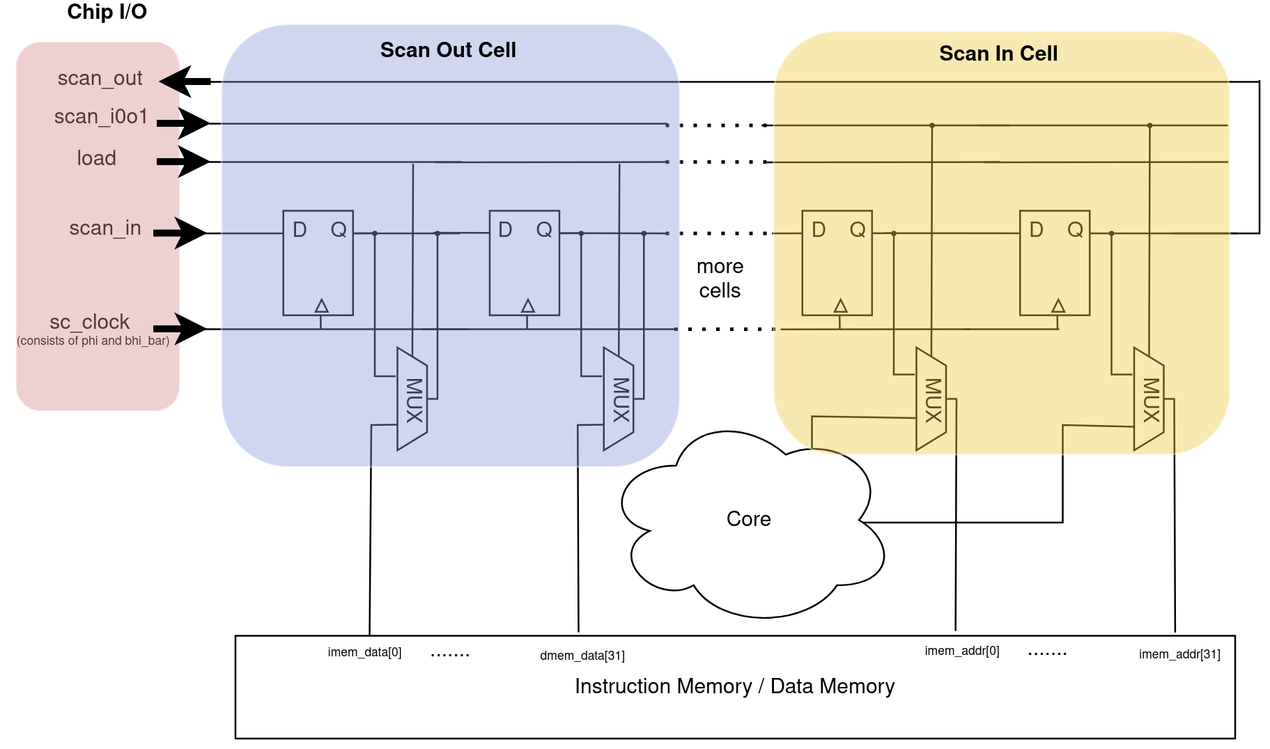
In total, the scan chain consists of 248 cells. Although for simplicity the diagram shows different scan-in and scan-out cells, in reality each cell integrates both operations which are controlled by the scan_i0o1 input signal. As it can be seen, a multiplexer (MUX) is used to connect with the memory. For the clock generator and FSM connections no MUX is used. In practice, the MUX that is shown in the scan-in cell is part of the memory wrappers and only one MUX used for scanning out is part of the scan cells. Each cell is connected to an individual bit of the memory ports or the clock generator and FSM registers. For example, one cell is connected to the 5th bit of the instruction memory address port while the next cell is connected to the next, 6th, bit. Therefore, during scanning in it takes 248 cycles to load all cells with the appropriate data through the scan_in port. These data could be the 32-bit instruction memory address and the 32-bit instruction to be loaded to that address. To better explain the scan chain operation, a more detailed view of the scan cells is given in Figure 5 and Figure 6.
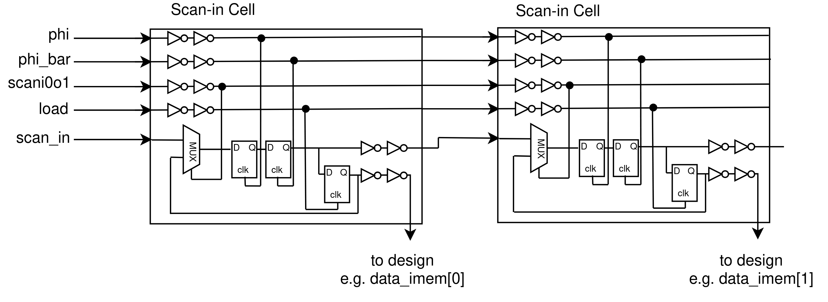
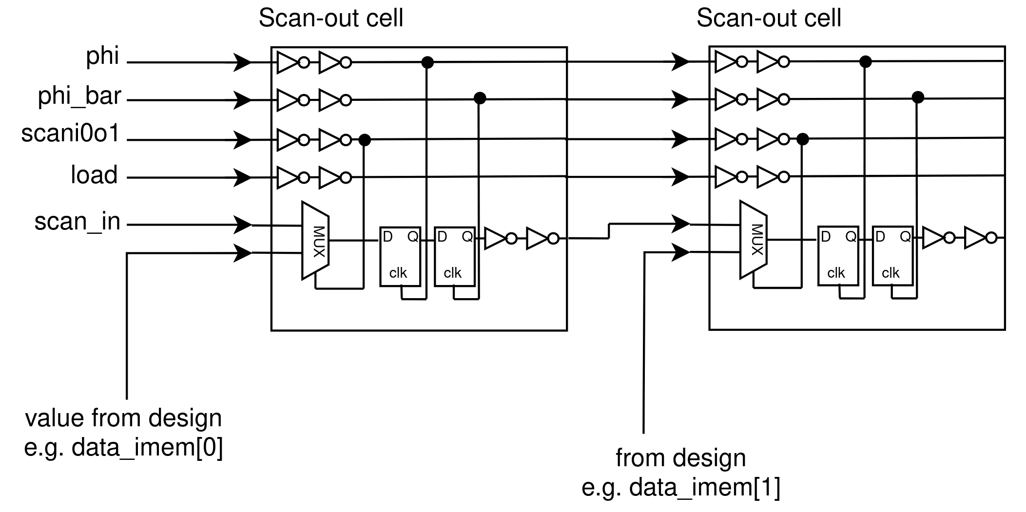
The scan chain deploys two back-to-back transparent latches in each cell and two non-overlapping clocks to ensure timing closure during scanning in and scanning out. It is known that shift registers can suffer from hold violations and thereby this design approach is necessary to ensure correct operation. As mentioned, during scan-in 248 cycles of the scan chain clock are required to load all cells with appropriate content and then one pulse in the load port is needed to load the flip-flops with these values. The output of these flip-flops are connected to one of the two inputs of the MUXs in the memory wrappers, while the other inputs are connected to the processor. During scan-in, an internal signal that controls these MUXs is kept high and therefore the Scan Chain is connected to the memory ports. During normal operation, this signal is kept low to enable the connection between the processor and the memories. This can be better understood by observing Figure 7, that shows a part of the interface between the Scan Chain, the processor and the Instruction Memory.
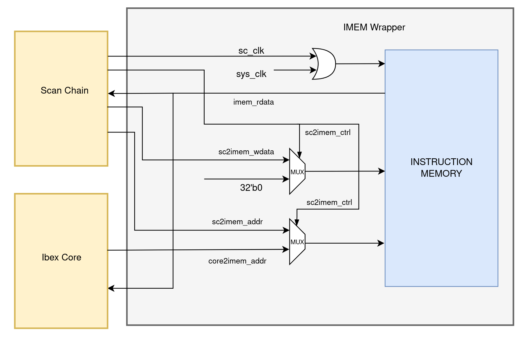
Once the flip-flop is loaded with the appropriate content, a rising edge to the memory's clock port is required. As shown, this port is driven by an OR gate that takes the general system clock and a "virtual" clock from the scan chain as inputs. During scanning in, the system clock is disabled as it will be explained in a later section and the sc_clk plays the role of the memory clock. This signal comes from a scan cell and to "simulate" a rising edge we need to force it low and then high. This means that it needs to be loaded twice, with two different values, which consequently means that the entire scan chain needs to be loaded twice with the same content in all cells except the cell that drives the sc_clk. As a result, to load 1 instruction to the instruction memory 496 cycles are required.
On the contrary, the scan-out process is relatively simpler. While the scani0i1 signal is set high, the MUX in the scan chains allows the contents of the memories to reach the transparent latches. After generating the appropriate number of cycles, the values of the desired registers are read out of the chip through a dedicated scan_out port which is connected to the end of the scan chain.
Clock Generator
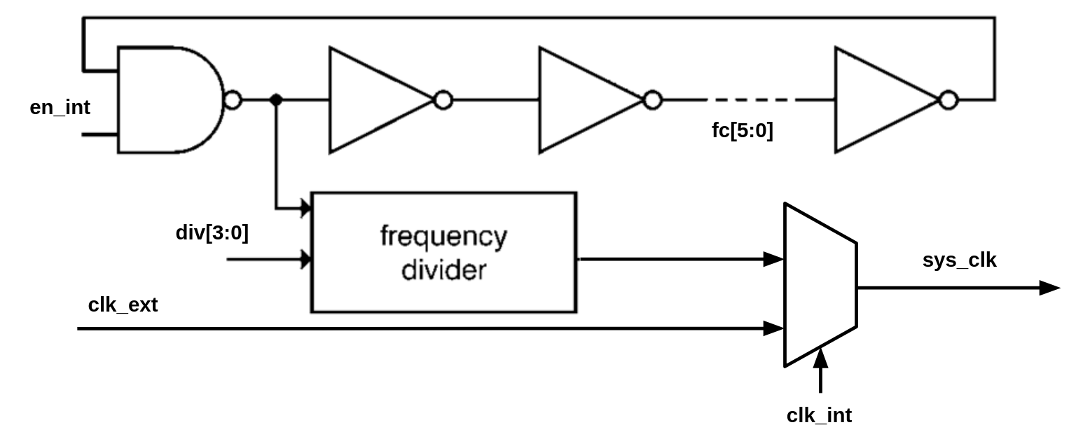
To be able to sustain high operating frequencies, an on-chip clock generator was used. A simplified diagram is shown in Figure 8. The clock generator can be runtime-programmable by the user through the div and fc registers, which together determine the generated clock period and are configured through the scan chain. The div value configures the frequency divider to select a coarse range of available periods, while fc selects the ring oscillator length for fine-grained/exact period determination. Additionally, the chip was designed to support the use of an external clock through the clk_ext input pin by setting the input pin clk_int to 0, to ensure the ability to operate correctly even if the internal clock generator malfunctions. The en_int is another parameter configured during setup through the scan chain and is set high when the internal clock is used.
Testing FSM
To enable fine-grained debugging of the chip after fabrication, a Finite State Machine (FSM) that implements some basic gating logic was used. Specifically, the FSM allows 3 different operation modes. During the use of the Scan Chain for scan-in or scan-out, the FSM is set to idle mode and it supress the input clock. For normal operation, it is set to running mode and allows the input clock (external or internal) to pass through. The most interesting case is when it is set to countdown mode, which enables the clock for a specific number of cycles, given as an input value, and gates it after. In this way, cycle-accurate debugging can be performed. Note that both the mode and the number of cycles to count are configured through the Scan Chain.
Communication Peripherals
The red-colored blocks at the left side of the block diagram implement the communication interfaces of the chip that are necessary to improve the use value of the processor and enable real-time interaction with the users.
AMBA AHB Bus & AHB-APB Bridge
Apparently, the fact that the CPU needs to communicate (send/receive data) with multiple peripherals (devices) makes the use of decoding logic necessary, to enable correct data transferring between the core and the desired device. For this reason, a bus compliant with the ARM AMBA AHB protocol was deployed. As shown in Figure 9, the bus is connected to the Data Memory Interface of the Ibex core and the Load-Store Unit constitutes the sole Manager of the configuration. On the other side of the bus, there are three Subordinates, the Data Memory, the General Purpose Input Output (GPIO) peripheral and an AHB-to-APB Bridge, that allows further communication with the Universal Asynchronous Receiver/Transmitter (UART) and Serial Peripheral Interface (SPI) modules. This bridge simply translates the AHB requests to APB-compliant messages to the appropriate device.
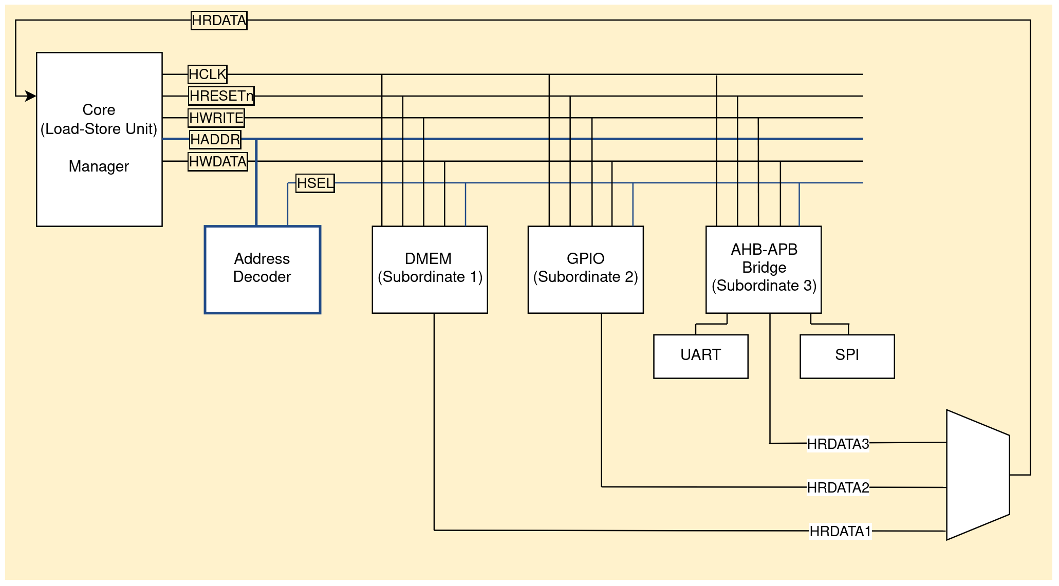
This implementation scheme requires the definition of a memory map, that determines the memory addresses that correspond to each Subordinate, since the processor issues the same read/write requests regardless of the destination, and therefore the decoding logic of the bus needs to select the desired device. The memory map of our implementation is described in Table 1. Although the Instruction Memory is not related to the bus decoding logic, it is included for completeness, and we will refer to it in the Software & Testing Flow section.
| Device | Start Address | End Address | Size |
|---|---|---|---|
| Instruction Memory | 0x100000 | 0x107FFF | 0x008000 (32KB) |
| Data Memory | 0x108000 | 0x10FFFF | 0x008000 (32KB) |
| GPIO | 0x200000 | 0x200003 | 0x000004 (1B) |
| UART | 0x300000 | 0x30000F | 0x000010 (16B) |
| SPI | 0x400000 | 0x4000A3 | 0x0000A4 (164B) |
GPIO
The GPIO module is probably the simplest part of the proposed chip and it is used to implement basic communication with the outside world, as it will be explained in the Demonstration section. On the output path, there is a simple register that is updated everytime a write request is sent from the bus. On the input path, a synchronizer consisting of two back-to-back registers is used to avoid metastability. When a read request is received from the processor, the output value of the synchronizer is sent to the bus.
UART
UART is an asynchronous serial communication protocol widely used for data transfer. For this project, we used the open-source UART developed by PULP [3]. This module is memory-mapped, and configuration of several internal registers is required before initiating any data transfer. These registers define essential parameters such as:
- Number of start bits: 1 bit
- Number of data bits: 5, 6, 7, or 8 bits
- Parity bit: 1 bit (optional)
- Number of stop bits: 1 or 2 bits
The registers that need to be configured before data transmission are the following:
DLLandDLM: Divisor registers for baud rate configurationIER: Interrupt Enable RegisterLCR: Line Control Register for data format configuration (e.g., parity, stop bits)LSR: Line Status Register for TX status reporting
Although we do not provide a detailed description of the module's microarchitecture, since it is open-source, it is important to mention that it consists of two main components. These are the UART_TX block, an FSM that handles data transmission, including the start, data, optional and end bits, as well as the baud rate generation through a counter, and the UART_Interrupt block, which manages the UART interrupts by determining their causes and generating interrupt signals to the processor. Note that in this project, only the output functionality of the UART protocol is used.
SPI
Similarly to the UART peripheral, an open-source SPI module with APB interface developed by the PULP group [4] was deployed for the purposes of this project. This module has an interface with the outside world, which consists of following 4 primary ports:
- SPI Clock (Output): Synchronizes communication
- SPI Chip Select (Output): Selects the target device
- MOSI (Output): Transmits data to the device
- MISO (Input): Receives data from the device
Similarly to the UART peripheral, only the output functionality of the SPI protocol is used. The module used integrates a controller, that is an FSM that orchestrates the block's operations, including the SPI clock generation, and a FIFO, that stores outgoing data. Before data transmission starts, the following SPI registers need to be configured:
REG_SPILEN: Defines the number of bits for command, address, and data. In our system, the length of each of them is set to a byteREG_CLKDIV: Sets the SPI clock frequency by dividing the system clock.REG_SPICMD: Stores the command to be transmittedREG_SPIADR: Stores the address to be transmittedREG_TXFIFO: Holds data for transmission, which is transferred through the transmit FIFOREG_STATUS: Activates the SPI clock and initiates data transmission