
PCB Design
As part of the class project, for the Demonstration, a PCB (Printed Circuit Board) had to be designed that would integrate our RISC-V chip as well as any devices that would communicate with it through its communication interfaces. An overview of our PCB is given in Figure 25.
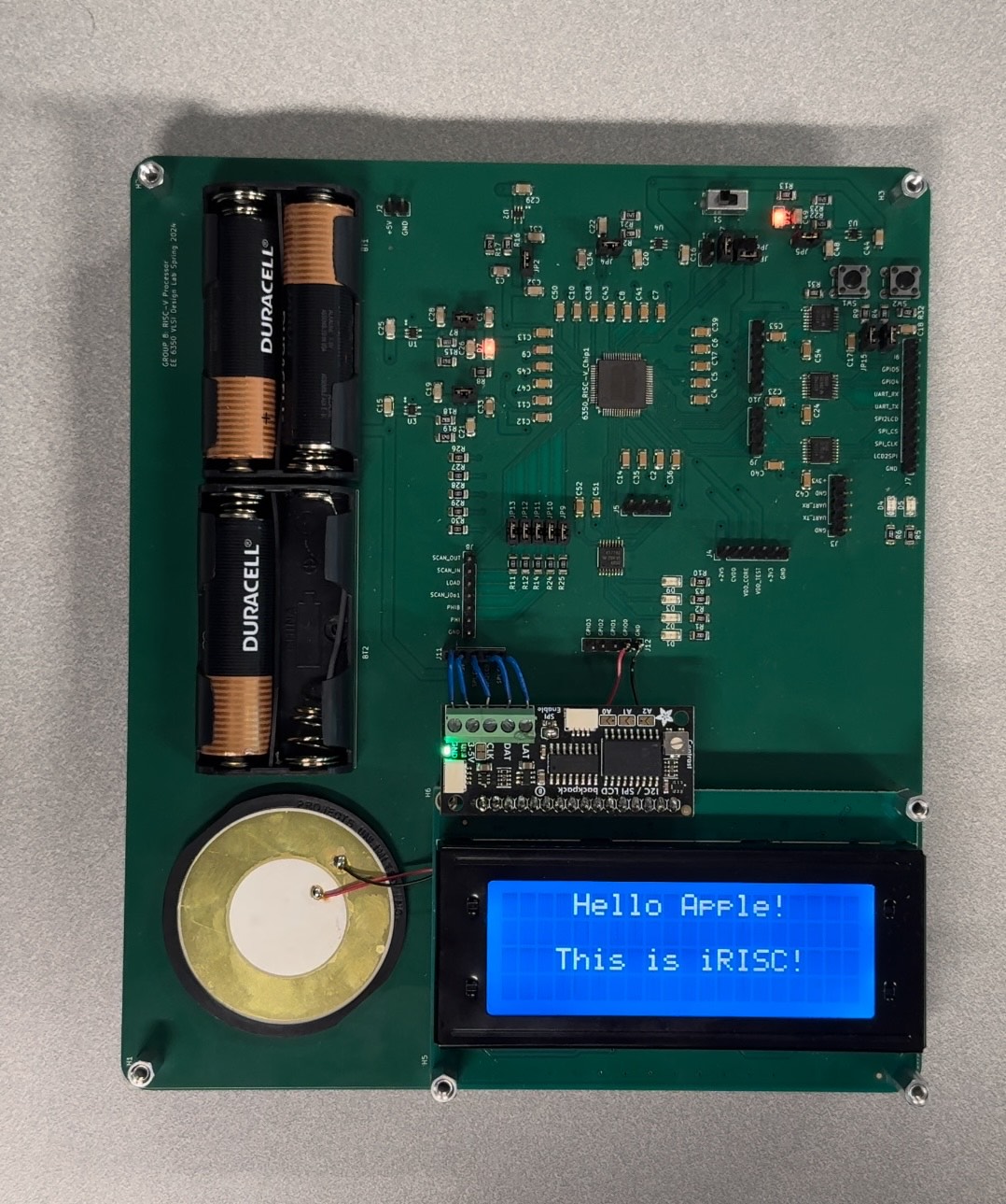
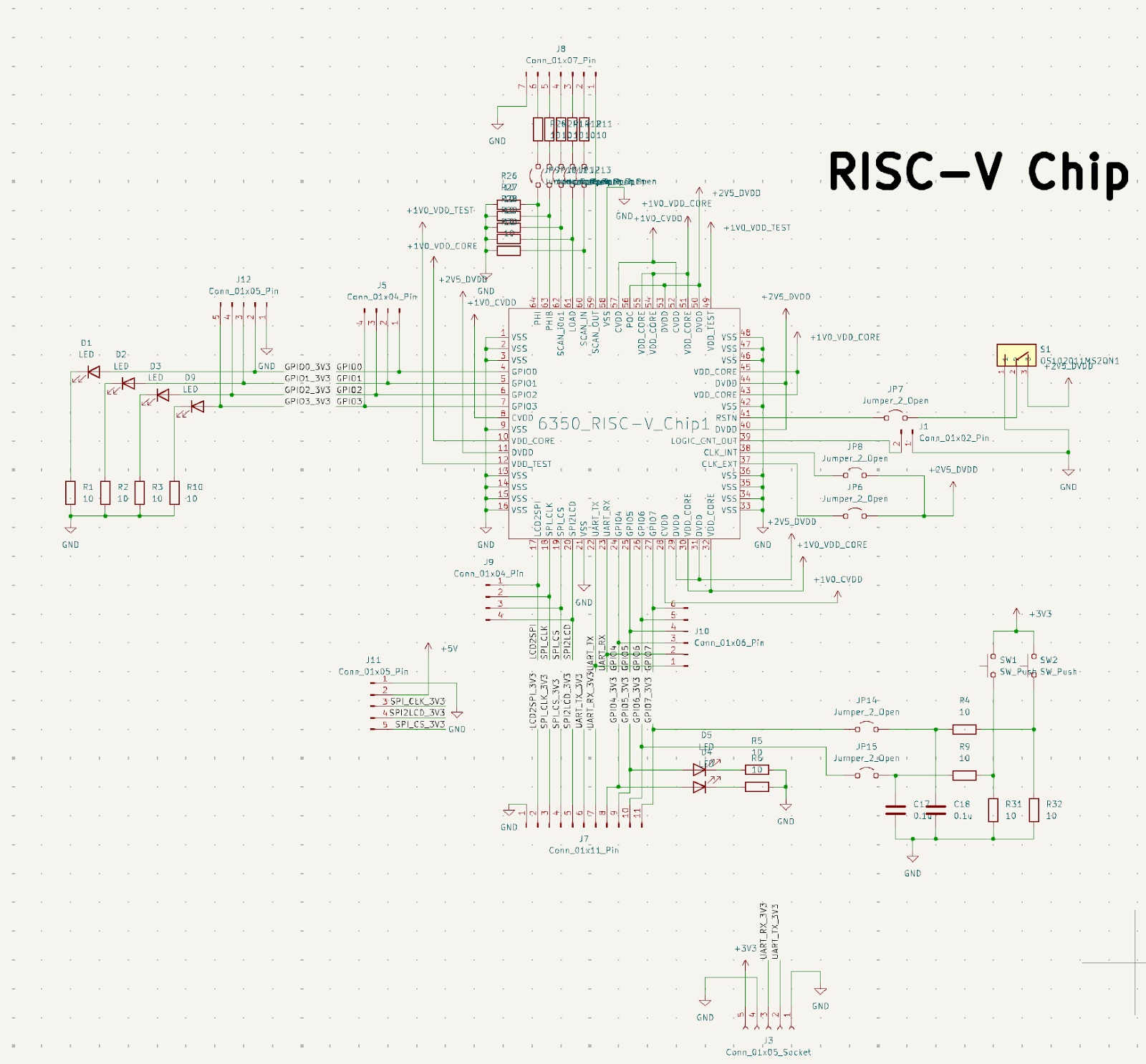
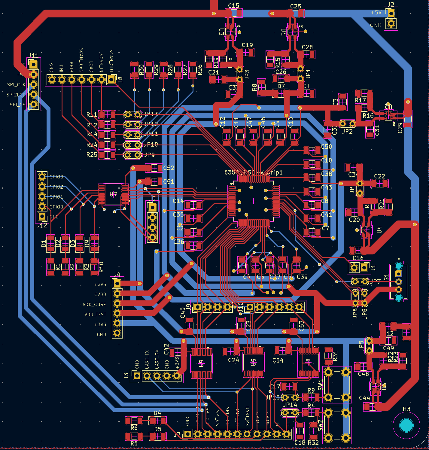
The PCB has 5 main parts: the power supply, the decoupling capacitors, the level shifters, the RISC-V chip and the external devices. The overall PCB schematic and PCB layout are given in Figure 26 and Figure 27 respectively.
Power Supply
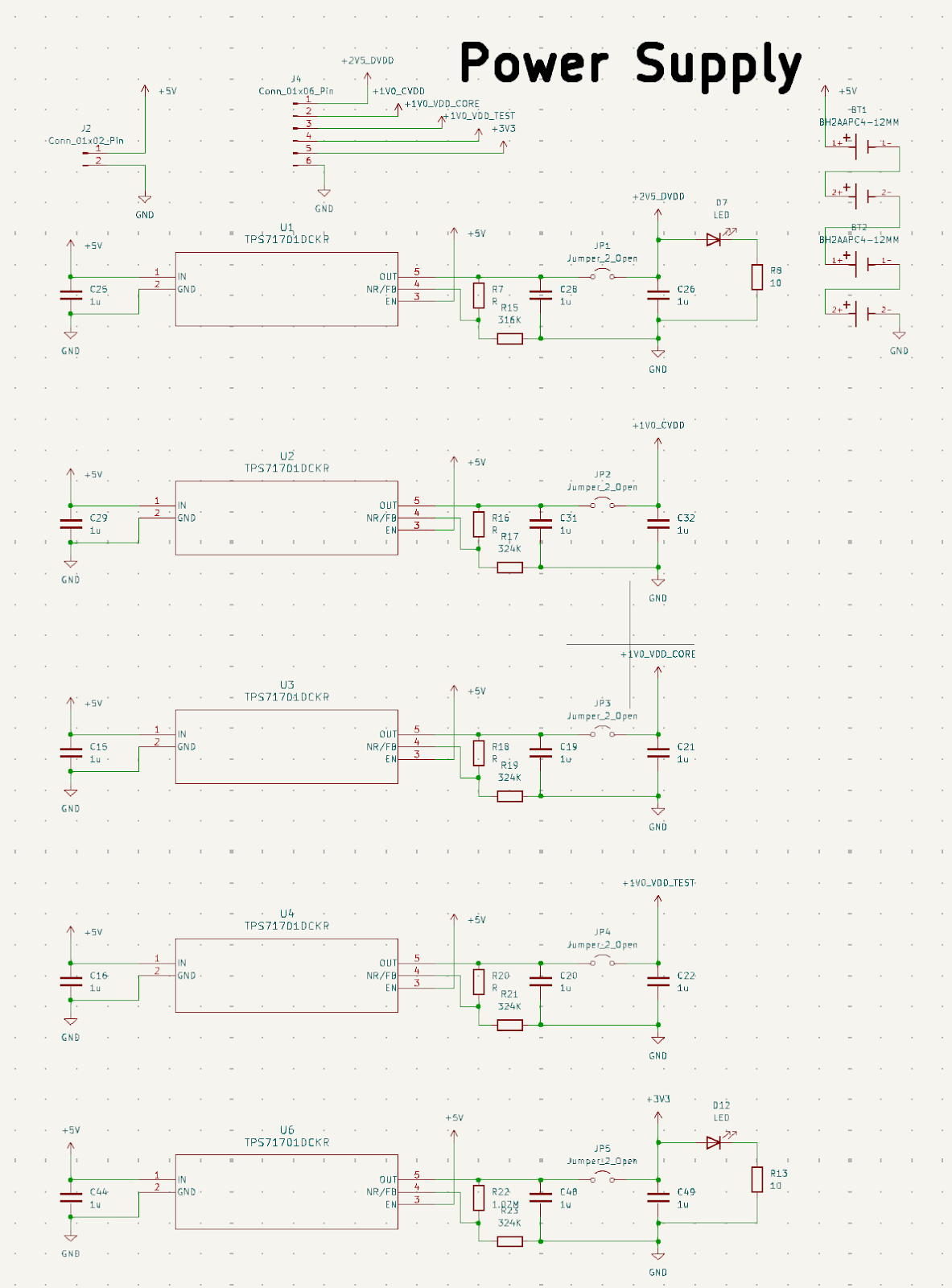
Our primary power source are batteries. While the batteries are nominally rated at 1.5V, testing indicates a typical voltage of approximately 1.65V, prompting the use of three batteries in the design. The PCB requires three distinct voltage levels: 2.5V and 1V for the chip, 3.3V for SPI and UART. To meet these requirements, a variable LDO was chosen for the power supply. The output voltage is set by the values of the feedback resistors. Test points are incorporated to facilitate measurement of the LDO's output during testing. Additionally, two LEDs are included to provide visual indicators for the 2.5V and 3.3V power outputs. Apart from the batteries, the PCB can also be powered through 5V and GND pins on the board. The schematic of the power supply is given in Figure 28.
Decoupling Capacitors & Level Shifters
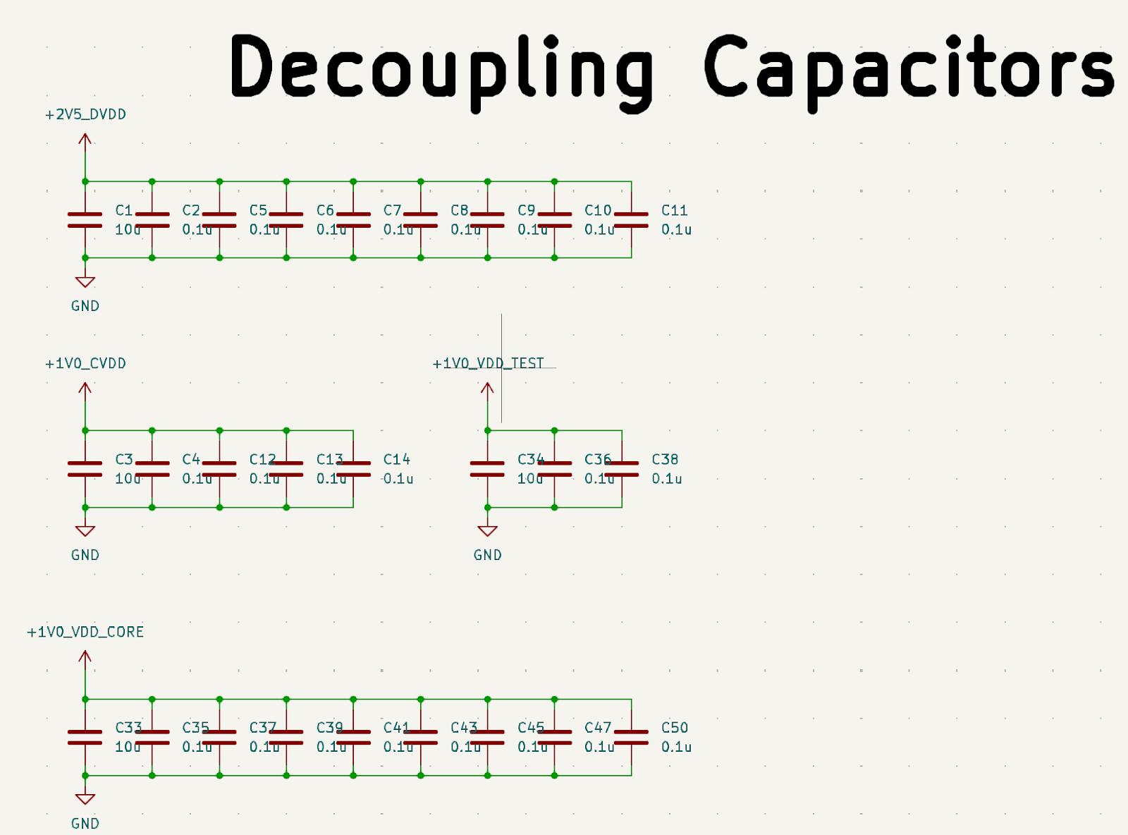
Decoupling capacitors were added to ensure a stable and clean power supply to the chip. Each power domain of the chip is equipped with a 10 µF capacitor, while each input power pin is provided with a 1 µF capacitor. The relevant schematic is given in Figure 29.
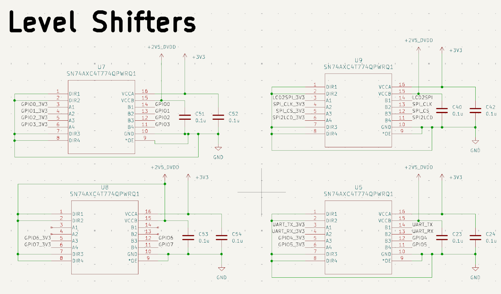
Since our peripherals mainly support 3.3V I/O voltage, level shifters have been incorporated into the chip's I/O to convert the 2.5V I/O voltage to 3.3V. The schematic of the level shifters is given in Figure 30.
RISC-V Chip
As the chip is programmed using an Arduino, which operates with a 5V output, a voltage divider is added for the scan chain pins to ensure proper voltage levels. Additionally, a switch is integrated into the PCB to facilitate chip reset functionality. As shown in the PCB overview, the input GPIO pins are driven high when the respective buttons on the PCB are pressed. The output GPIO pins drive 6 LEDs and a piezo element to be used as a speaker during the demonstration. The UART interface corresponds to two pins on the board that can be connected to a PC to output values on a terminal, however, the UART RX is not functional with our chip. Finally, the SPI interface drives an LCD screen. Once we knew which LCD screen would work for us, we created free space on the PCB to mount it directly on it, with the SPI ports at the same spot to conveniently connect the display as part of the PCB.