
Software & Testing Flow
An essential part of our project was the integration of the RISC-V software flow, that was used for both RTL verification and post-silicon validation and testing. A high level flow diagram of this process is given in Figure 23.
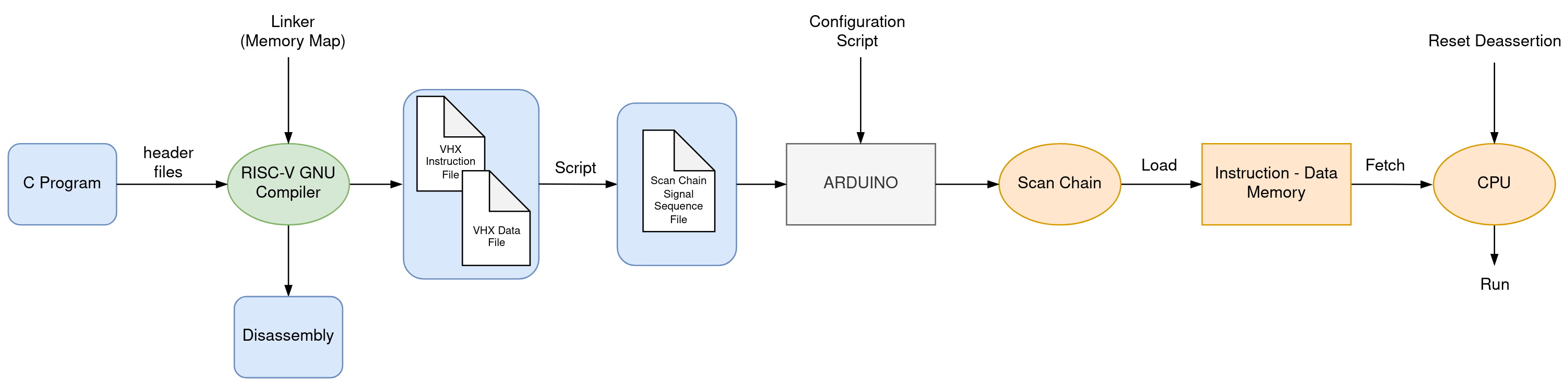
The first step requires the user to write a C program that can be compiled by the 32-bit RISC-V GNU Cross-Compiler used. The compiler takes as input the C program together with some necessary header files that contain common C functions and functions related to interrupts and UART. The linker file also contains essential information regarding the memory map and what addresses correspond to data and instruction memory. The information provided by the linker needs to follow the memory mapping that was used during hardware design and explained in the System Architecture section.
More specifically, the instruction memory layout starts with the interrupt vectors (.vectors section) which take up 84 addresses. After that, the .text section which contains the actual compiled instructions starts. At the end of the instruction memory, the data memory starts, at address 0x108000. The data memory contains the .rodata section, which holds read-only constant data, the .data section that holds initializes variables and the .bss section that holds uninitialized data. The size of each section depends on the compiled code. At the end of these section, the stack is located, where auto variables are dynamically stored. Our linker specifies that the minimum length assigned to the stack should be 8KB.
The compilation of the C program generates an ELF image file that can be used to generate VHX files (Verilog Hexadecimal Format) for instruction and data. A VHX file is a text file that contains the words (i.e. 32-bit) of instructions or data in the order they need to be stored in the system's memory in hexadecimal format. In practice, the generated file is slightly modified with a Python script to hold one 32-bit word per line. This file can be used as the source file in a testbench to load the memory modules. In RTL simulation, these files were read line by line and their values (and respective addresses) were loaded in the memories through the scan chain. The compiler can also produce a Disassembly file, which maps each binary instruction to the corresponding assembly instruction generated by the C program. This file can be used for understanding and debugging. Figure 24 demonstrates this software flow for a simple C program.
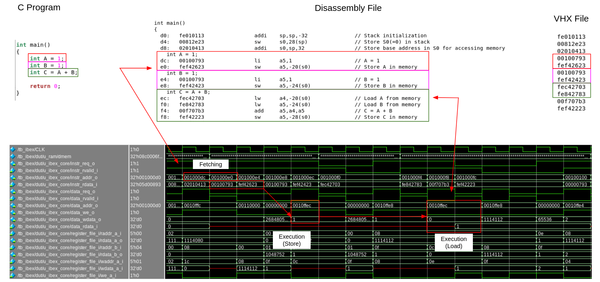
Initially, one can see how the C program generates the Disassembly file and how each hexadecimal number (instruction) is also present in the VHX file, without additional information. Once the VHX file is loaded and the processor is running, in RTL simulation we can see that the processor sends an address to fetch an instruction from the memory and then that the instruction shown in the VHX and Disassembly files is returned and executed. This process was used throughout the design phase to verify all components, such as GPIOs, UART and SPI. Note that part of the verification process was to use the Scan Chain to read out values from expected addresses through the scan_out port.
Chip Validation & Testing
To validate the correct functionality on the fabricated chip, this process had to be brought out of the RTL testbench to the real world, meaning that the actual chip pins of the Scan Chain had to be driven in the correct way to load the memories. After multiple iterations we optimized this process by using an Arduino UNO microcontroller. Initially, a script was needed to configure the microcontroller's pins to operate as desired, that is as outputs to drive the Scan Chain pins. The most important component of this process is a Python script that takes as input the VHX files and generates the appropriate drive values of all Scan Chain pins for each clock cycle. We mentioned in System Architecture that 496 cycles clocks are needed to load one instruction to the on-chip memory. Since these cycles refer to the two-non overlapping clocks, that means that one cycle is a sequence of 4 steps, one that both clocks are low, one that first clock is high and the second low, one that both are low again and one that the first clock is low and the second is high. The script is responsible for generating every such step for every instruction in the VHX file. As a result, every instruction (line in the VHX file) corresponds to 4x496 lines in the output Signal Sequence File. Once this file is generated, its contents are sent through the PC UART to Arduino, which parallelizes them in groups of 5 (5 output pins to the Scan Chain) and toggles its configured pins accordingly. At the end of this transferring process, the memories are loaded with the appropriate content and the processor can start running after deasserting the reset signal.
Code reference
Here you can find all the code that we used to generate the scan chain data and scanning them in. Note that some dependencies are missing as they were used in curtesy of Prof. Mingoo Seok.