Chip Specifications
The specifications of our chip are summarized in Table 3.
| CPU Architecture | RISCV32IMC | |
| Memory (SRAM) | 32KB Data | |
| 32KB Instruction | ||
| Peripherals | GPIOs | 2 Input & 6 Output |
| UART | Output | |
| SPI | Output | |
| Programming Interface | Scan Chain | 5 Input & 1 Output |
| Power Domains | VDD CORE | 1V |
| VDD TEST | 1V | |
| VDD IO | 2.5V & 1V | |
| Maximum Frequency | ~140MHz | |
| Power Consumption (60MHz) | ~40mW | |
| Die Size | 2mm2 | |
| Transistor Count | ~500,000 | |
Testing revealed that the maximum frequency at which the processor operates correctly is around 140 MHz. As mentioned in section Design Flow, the expected critical path after APR was 8.83ns which corresponds to a maximum frequency of around 113 MHz. We assume that this discrepancy is due to the pessimistic approach that Primetime adopts during STA.
During the debugging process, we also applied multiple configurations to the Clock Generator to understand what frequencies could be generated on real silicon. The applied configuration parameters and the respective clock frequencies are given in Table 4, which shows that the minimum and maximum frequencies are 9.34 kHz and 1.52 GHz respectively.
sc_clkgen_div |
sc_clkgen_fc |
Frequency (Hz) |
|---|---|---|
| 1111 | 11111 | 9.3424K |
| 1111 | 01010 | 20.682K |
| 1111 | 00101 | 29.361K |
| 1110 | 01010 | 41.358K |
| 1110 | 00101 | 58.685K |
| 1101 | 01010 | 82.672K |
| 1101 | 00101 | 117.35K |
| 1100 | 01010 | 165.43K |
| 1100 | 00101 | 234.80K |
| 1011 | 01010 | 330.69K |
| 1011 | 00101 | 468.87K |
| 1010 | 01010 | 661.38K |
| 1010 | 00101 | 938.44K |
| 1001 | 01010 | 1.321M |
| 1001 | 00101 | 1.877M |
| 1000 | 01010 | 2.637M |
| 1000 | 00101 | 3.765M |
| 0111 | 01010 | 5.252M |
| 0111 | 00101 | 7.530M |
| 0110 | 01010 | 10.593M |
| 0110 | 00101 | 15.010M |
| 0101 | 01010 | 21.552M |
| 0101 | 00101 | 30.02M |
| 0100 | 01010 | 42.264M |
| 0100 | 00101 | 59.98M |
| 0011 | 01010 | 84.414M |
| 0011 | 00101 | 119.66M |
| 0010 | 01010 | 168.83M |
| 0010 | 00101 | 239.46M |
| 0001 | 01010 | 336.75M |
| 0001 | 00101 | 476.74M |
| 0000 | 01010 | 669.16M |
| 0000 | 00101 | 946.97M |
| 0000 | 00000 | 1.524G |
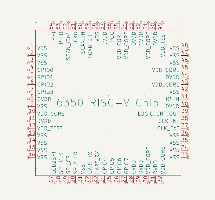
From the above frequencies, for the demo we ran the chip at 59.98 MHz, as this frequency made easier the synchronization of the UART peripheral at baud rate of 57600 The final chip pinout is shown in Figure 38.