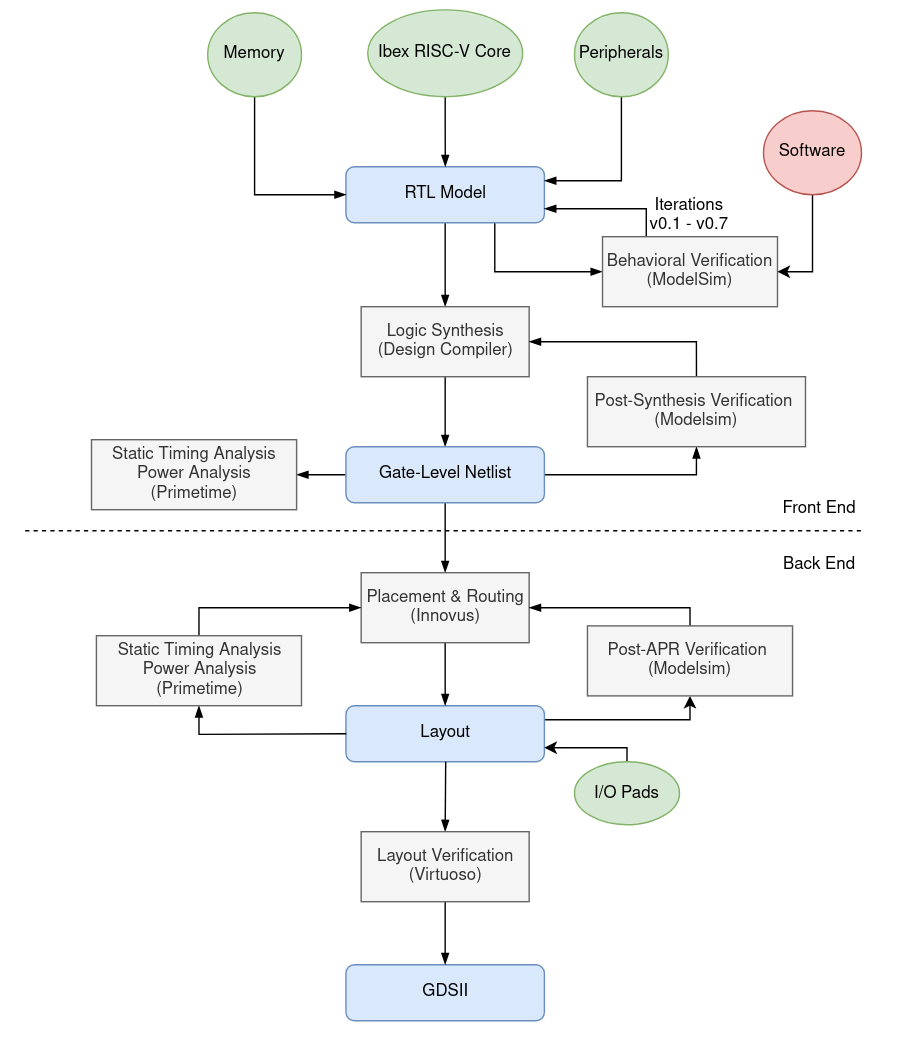
Design Flow
During the design phase of the proposed System-on-Chip we followed the complete digital design methodology, consisting of both frontend and backend flows, as shown in Figure 10. Our flow deployed a mix of CAD tools from different vendors, such as Cadence, Synopsys and Siemens.
Front End Design
During the front end phase of the design process, most of the time was spent on system integration and functional verification. To build our final system we followed an incremental approach of multiple iterations, as shown in Table 2. To understand the processor's architecture and functionality we started with the Simple System [5] example provided with Ibex by lowRISC, which makes use of a simple memory model and behavioral bus model. Following that, we incrementally added all the modules mentioned to complete our System-on-Chip. The software infrastructure required for RTL verification is explained in the Software & Testing Flow section.
| Version | Feature |
|---|---|
| 0.0 | Basic Model from lowRISC |
| 0.1 | Integrated SRAM with memory wrappers |
| 0.2 | Integrated AHB Bus |
| 0.3 | Integrated Scan Chain |
| 0.4 | Integrated GPIO |
| 0.5 | Integrated UART |
| 0.6 | Integrated Clock Generator |
| 0.7 | Integrated Pad Frame and IO Cells |
| 0.8 | Integrated FSM and increased memory size |
| 0.9 (Final) | Integrated SPI |
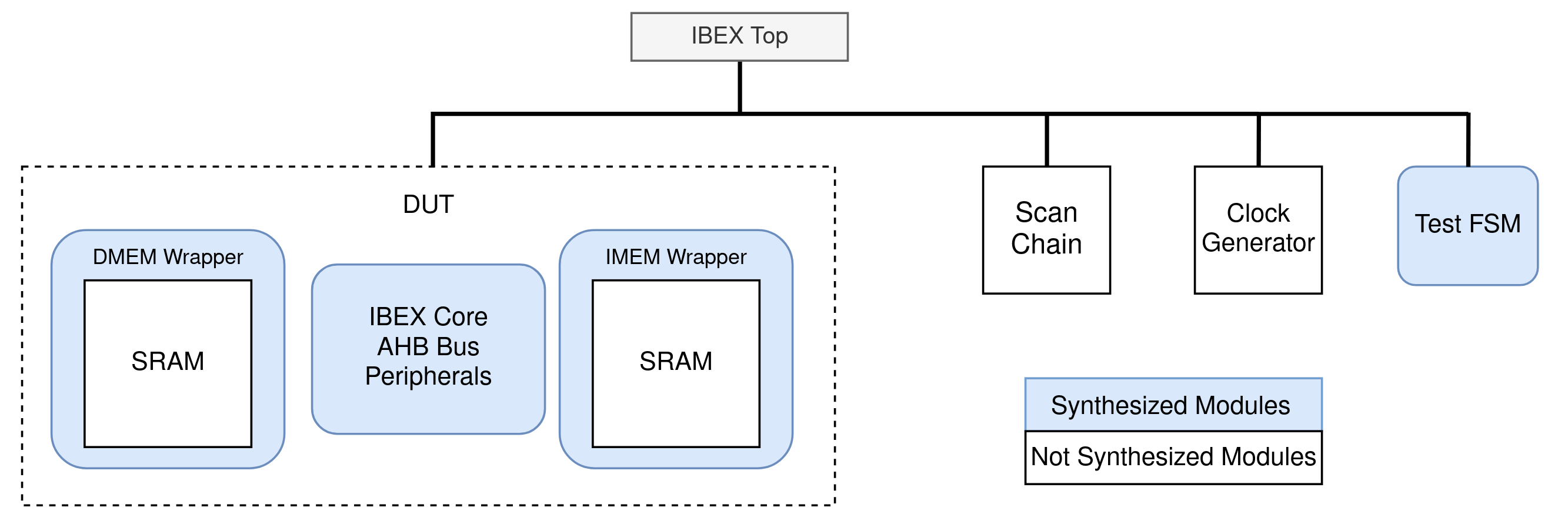
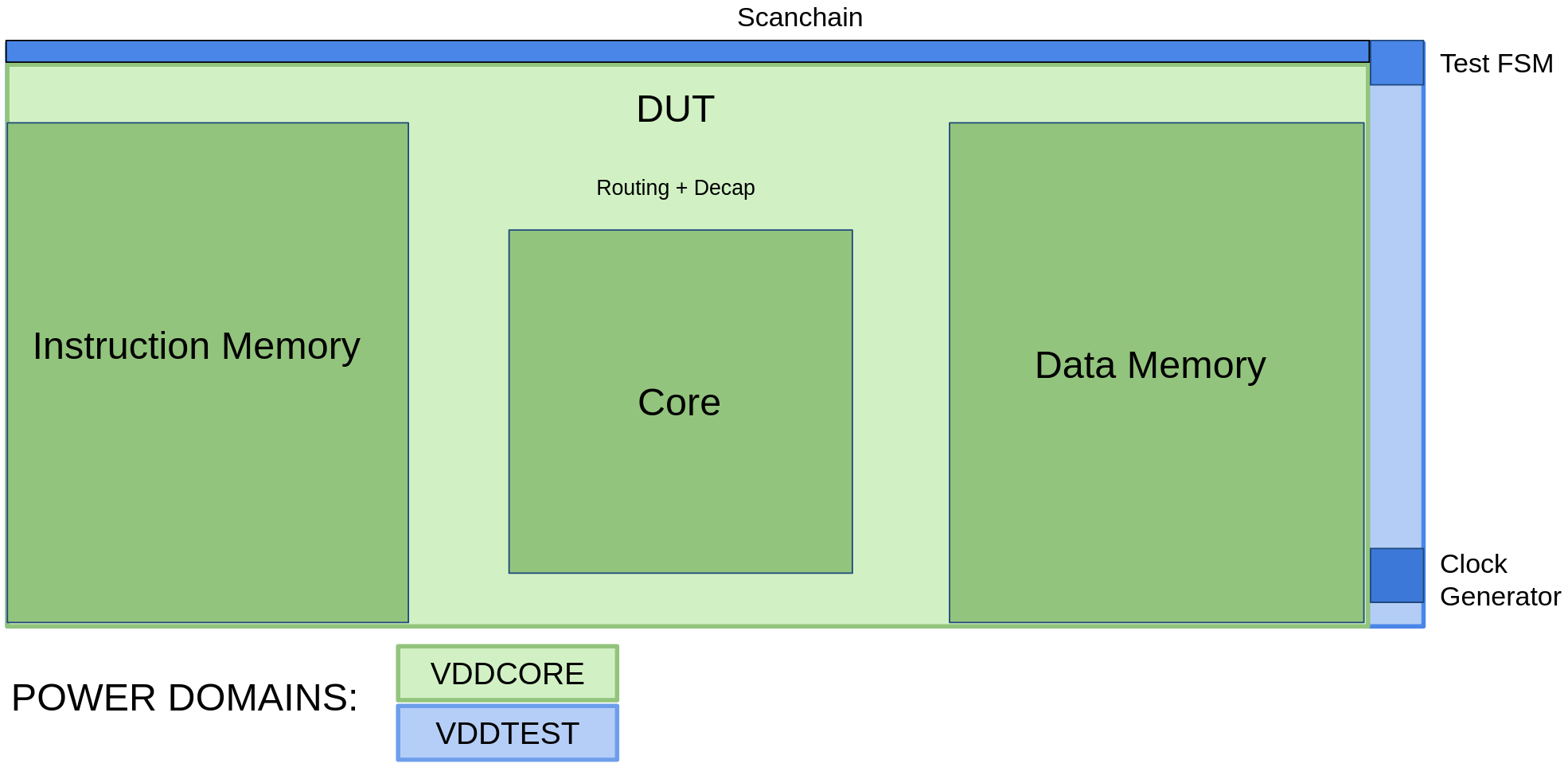
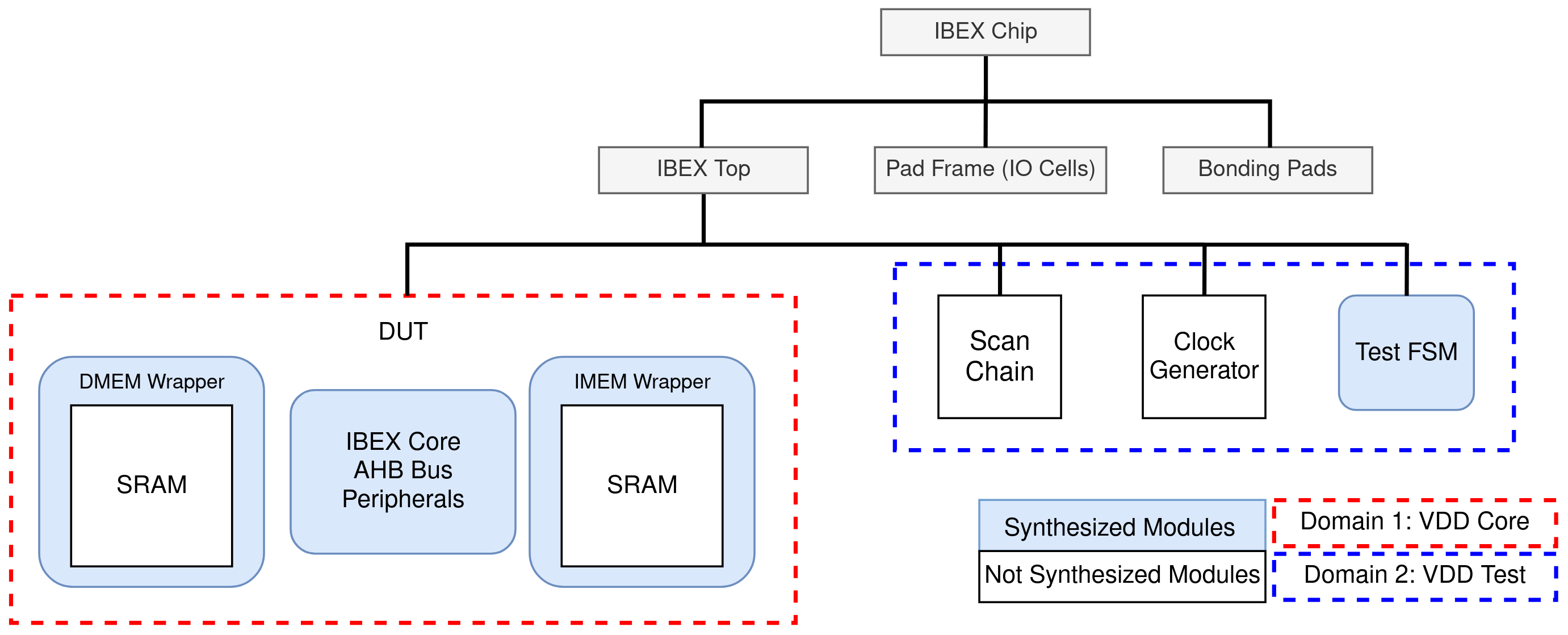
To ease the backend steps of Placement and Routing, during Synthesis we followed a modular approach, where every major submodule was synthesized separately, as presented in Figure 11. In particular, the Ibex core, the AHB bus, the communication peripherals and the designed memory wrappers were grouped together and synthesized as the Design-Under-Test (DUT). Note that the actual memory modules were not synthesized but they were only instantiated in the RTL description of the wrappers, since the memory compiler provides the final GDS files for them. Outside of the DUT sit three more modules, the Scan Chain, the Clock Generator and the FSM. The first two were implemented by directly using standard cells and were not described behaviorally in RTL. This is because they play an important role in the chip's functionality and we could not afford any optimizations on them by the compiler. Considering that the scan cells are "not touched" by the tools, each cell contains a buffer (back-to-back inverters) in every data line, to ensure sufficient driving strength, steep edges and timing closure, since each line may be travel over long physical distances on the chip. The FSM was synthesized alone, and together with the DUT, the Scan Chain and the Clock Generator they form the TOP module, as shown in Figure 11.
Synthesis was executed on Synopsys Design Compiler. The design was synthesized for a targer frequency of 100MHz and the tool was able to achieve a critical path of 5.21 ns. According to the generated reports the critical path is located in the heart of the processor, that is it is made up of a long logic chain within the IF and ID/EX stages. It is important to highlight that in order to clear setup violations we had to experiment and finetune the synthesis parameters in the tool scripts.
Back End Design
Most of the development time was spent on the back end phase, for layout optimization, timing closure and solving the errors flagged by the CAD tools.
Floorplanning, Placement & Routing
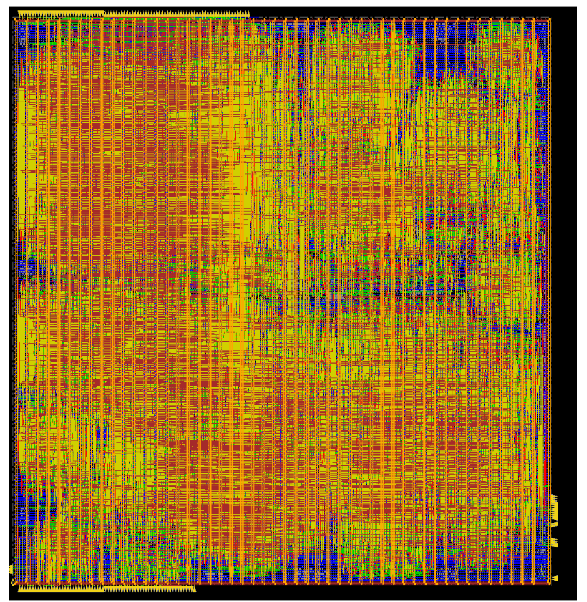
Following Synthesis, the modules that were synthesized separately were the components that had to be placed and routed as separate units. For this step we used Cadence Innovus and the final layout of the chip is given in Figure 12.
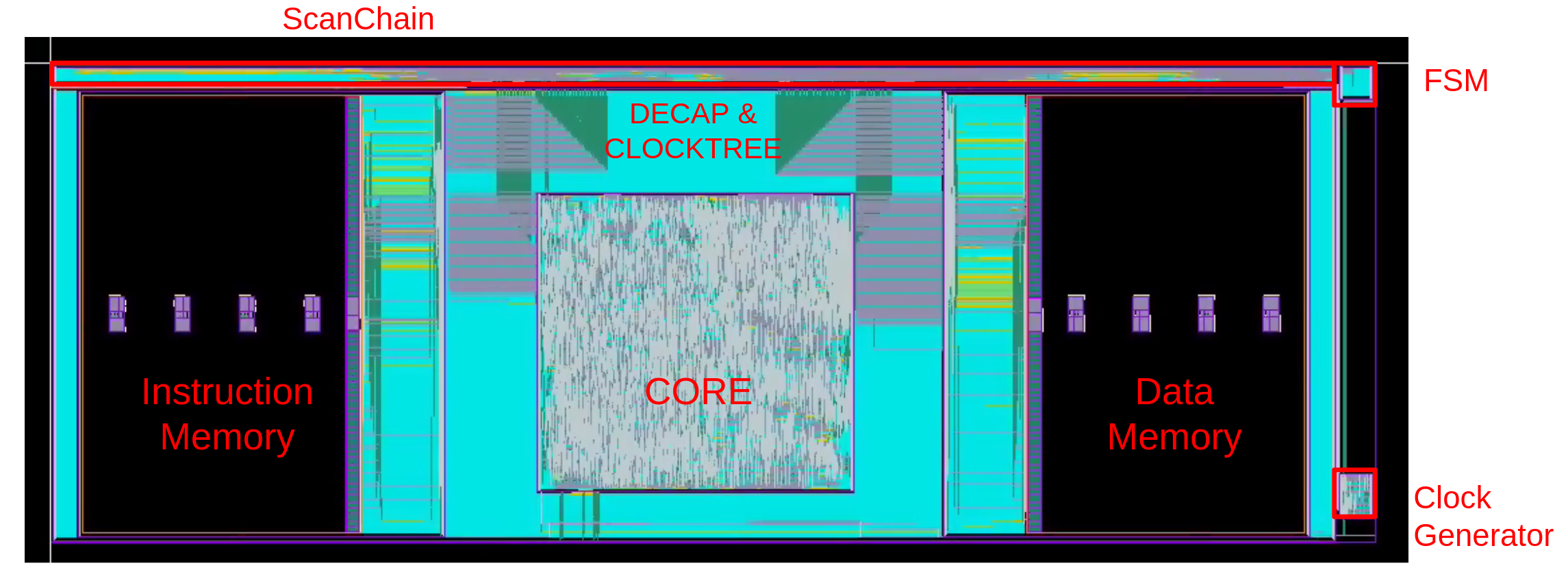
Our chip has an effective area of 2mmx1mm and in the middle of it sits the RISC-V core with the peripherals, that have been synthesized and placed/routed together. At its left and right the two memory wrappers and the actual memory modules are placed. Across the long edge of the chip, the scan chain is located. This scheme allows optimal routing as the wire lengths and the number of corners in routing are minimized. One can see how the memory ports are located very closely to the core and the scan chain. The FSM and the Clock Generator are located at the corners of the chip, since their distance from the core does not really matter, as long as the distance is similar for all clocked objects (core and memories).
For learning and testing purposes after chip fabrication, we decided to divide our system into two power domains, namely VDD Core and VDD Test. A floorplan view of the design indicating the two power domains is given in Figure 13. Although two domains have been created, both of them are nominally running on 1V and they are only supposed to differ by a small value and therefore no voltage converters need to be inserted. The purpose of using two domains is that after fabrication, the blocks belonging in the different domains can be tested independently and thus debugging becomes easier, especially in cases of bug existence in silicon.
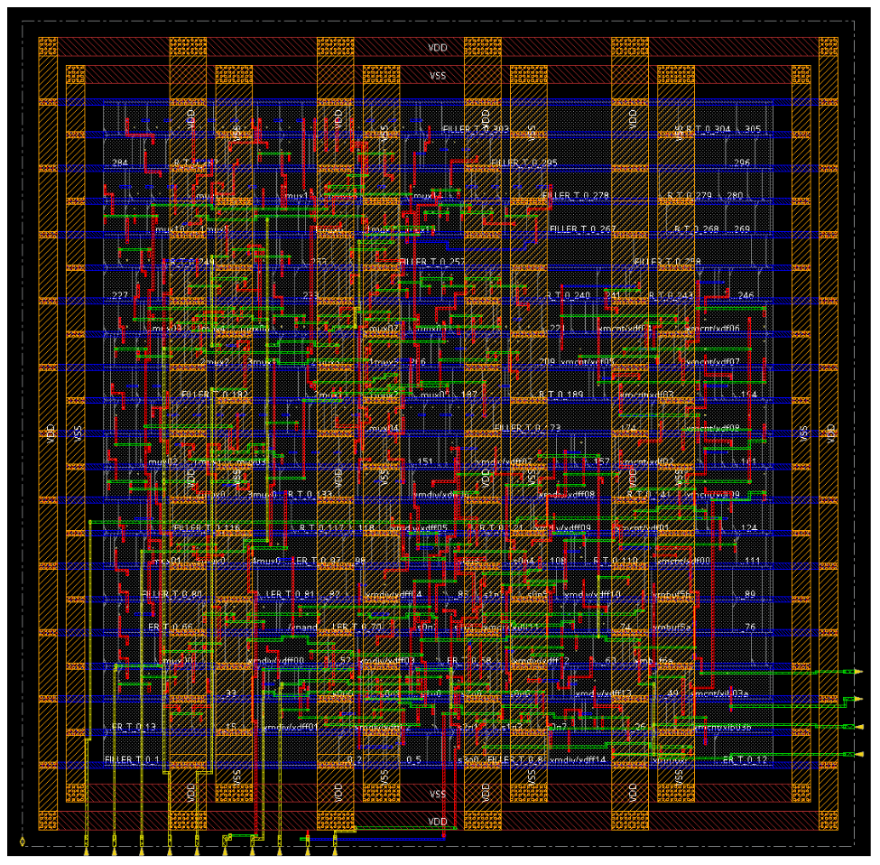
The first step during the backend phase was to place and route every component separately. The layout of the CPU and the peripherals is given in Figure 14. The achieved density was 72% and 49pF of decoupling capacitance was added.
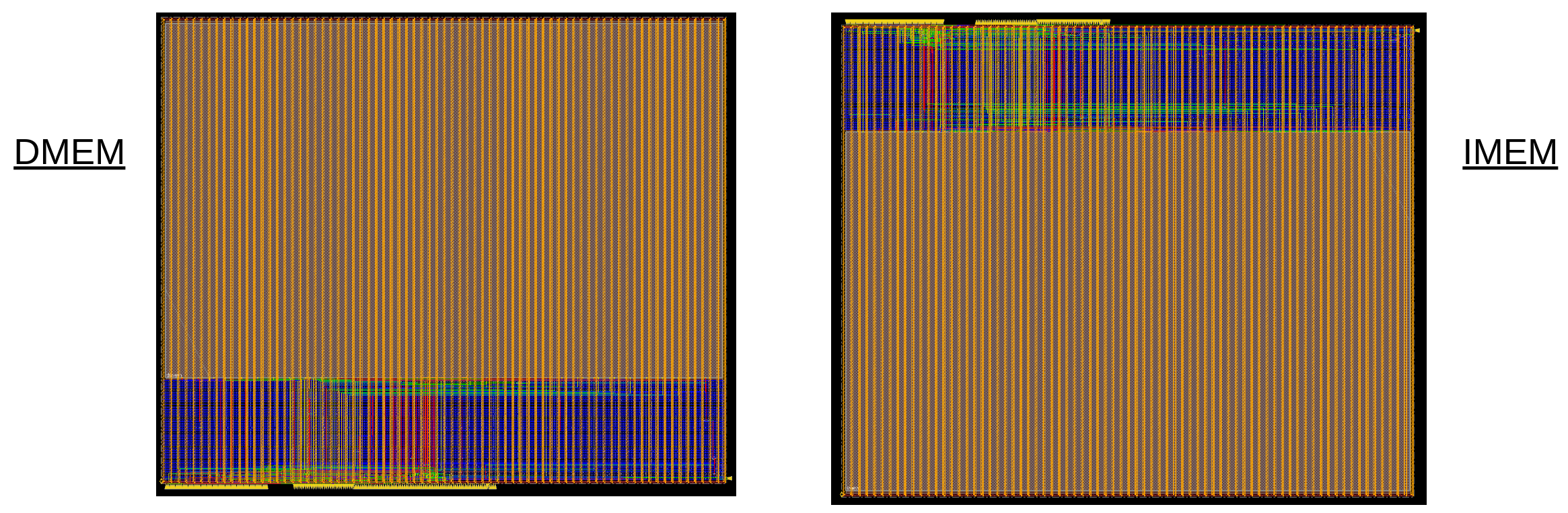
Similarly, the memory wrappers were implemented separately and the memory modules were assumed to be black boxes, since no netlist was used for them. The density of the memory wrappers was 77% and in total 300pF of decoupling capacitance was used for each of them. To ease routing in the floorplan presented, the Instruction Memory black box had to be flipped to have its ports facing the core. The respective layouts are given in Figure 15.
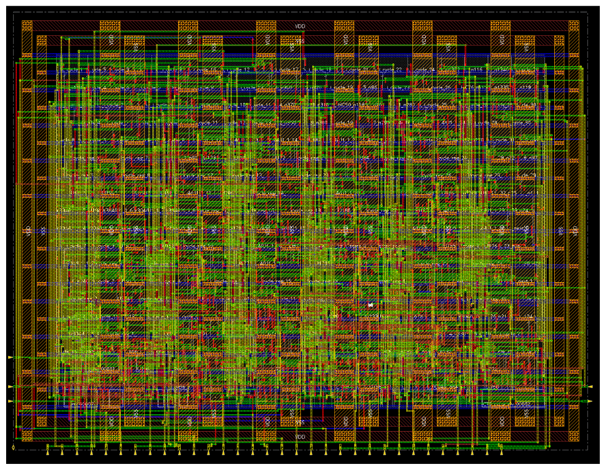
For the placement of the FSM, 60% of density was achieved and 1.5pF of decoupling capacitance was added while the respective numbers for the Clock Generator were 68% and 21fF. The layouts of these modules are given in Figure 16 and Figure 17 respectively.
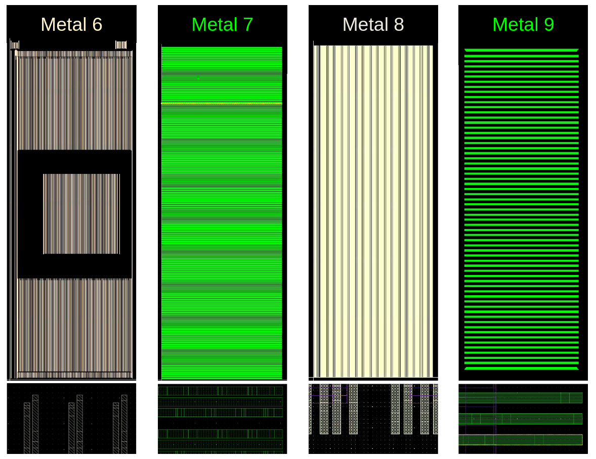
Once every component was placed and routed separately, placement and routing at the DUT and TOP levels took place. The standard cell density in both DUT and TOP levels was 73% and the added decoupling capacitance in DUT was in total 1.35nF. Before routing, the clock tree generation was performed at the DUT level of the design, which incorporated all effective modules of the design. In practice, every submodule (core and wrappers) has its own clock tree, and the clock tree generated at the DUT level is distributed to the submodules. The design technology used provided 9 metal layers (M1-M9), that were used for routing and power supply. M1 was used in the standard cells and in general M1 to M4 were used for routing within each module (e.g. core with peripherals). Then M5 and M6 were used for the power rings within the submodules, as shown in Figure 14, Figure 15, Figure 16 and Figure 17. The power stripes within the submodules were also implemented with M6. Power stripes at TOP level were implemented with M7 and M8. Lastly, M9 was used for power supply from the IO Pads to the TOP module. Figure 18 summarizes the above analysis.
For power estimation and timing analysis, we used Cadence Primetime and had to iterate multiple times over the synthesis and placement/routing steps to achieve sufficient results. In particular, detailed finetuning of the synthesis parameters was required to fix hold violations that were persisting after APR. Ultimately, we achieved a sufficient hold time slack of 0.32ns while the critical path at the final layout was calculated as 8.83ns and was located at the Control-Status registers component of the processor. The maximum total skew was determined to be around 0.03 ns, which is an acceptable value. Due to the clock architecture of the chip, some cells that are responsible for driving the clock are considered critical for correct implementation. These cells are the output cell of the FSM, which drives the clock to the DUT, the output cell of the Clock Generator and the OR gates in the memory wrappers that take as inputs the system clock and the "virtual" clock coming from the scan chain. According to the generated reports, all of these cells are sufficiently large and have sufficient driving strength.
The total decoupling capacitance added across all modules was around 2nF, with the majority of it being located withing the VDD Core power domain. With respect to power analysis, Primetime reports revealed a total power consumption of 11mW for test vectors covering a calculation intense task of matrix multiplication. This corresponds to 10mA of current supply, whereas each IO cell used can supply up to 80mA of current, meaning that the power requirements can be covered. The peak power seems to be significantly higher at 4.95W, with the memory modules being responsible for the 75% of it. The fact that this peak power corresponds to a very short time window during reset deassertion means that there is no safety issue regarding chip's operation.
I/O Pad Integration
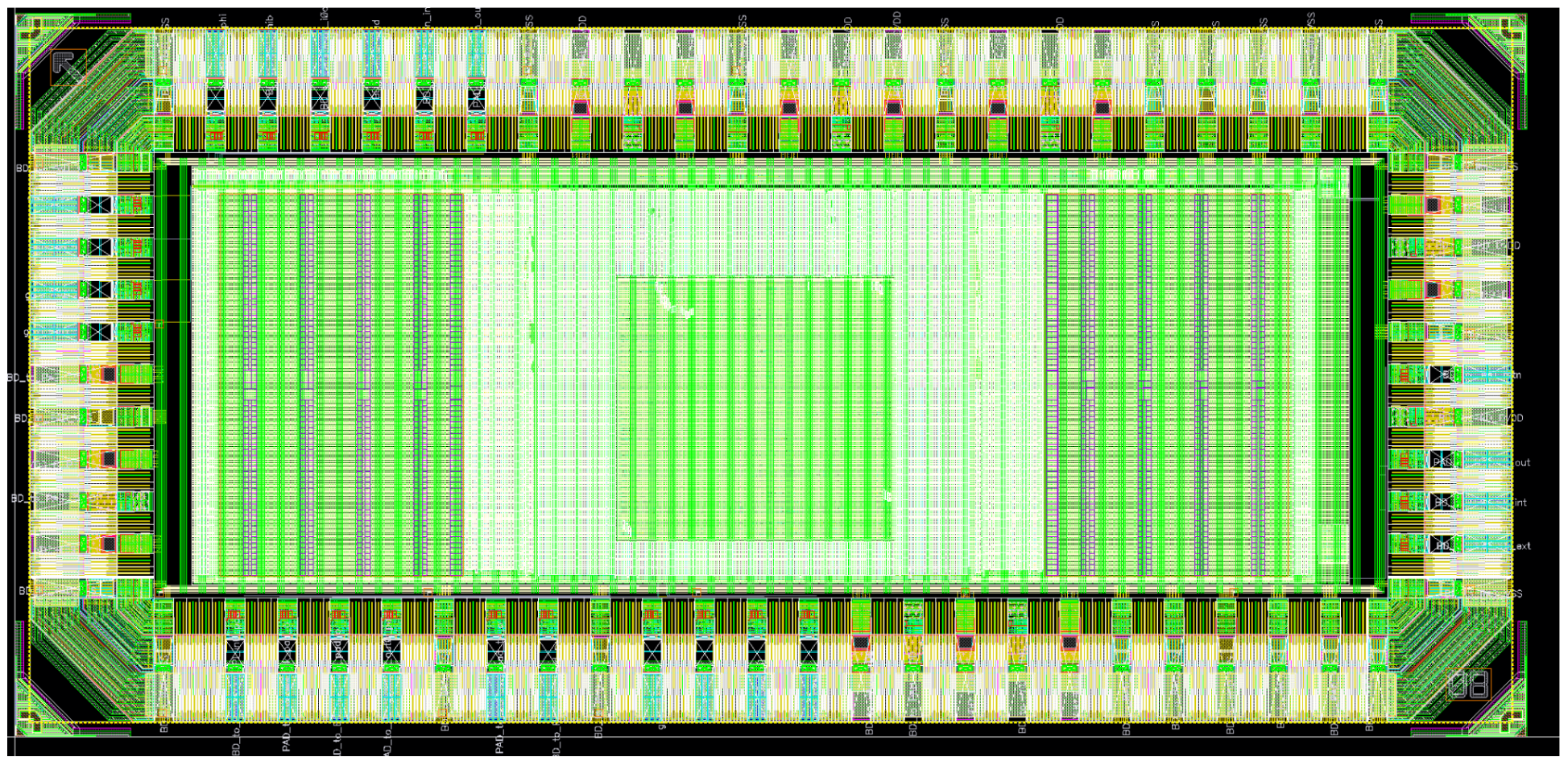
The last step in the design process was the pad integration with the TOP level of the chip. The final chip hierarchy, with the different power domains displayed is given in Figure 19.
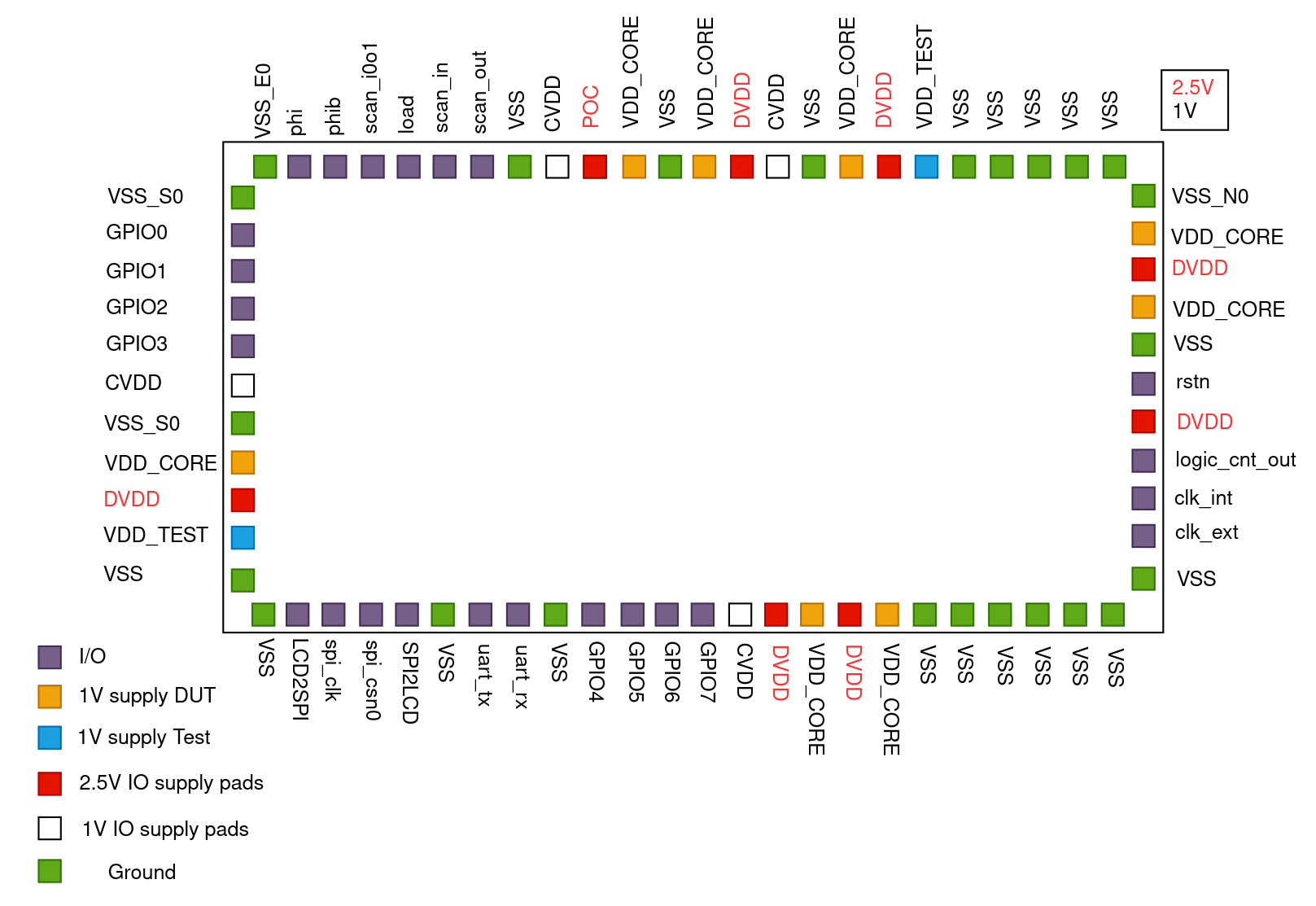
In our system for the I/O implementation we used TSMC standard I/O cells. We used analog power cells to supply both power domains, digital power cells to power the IO cells, input cells for all input pins, and output cells for all output pins. Using analog power for the core and test power domains was required to be able to vary the powers during debugging as discussed. We used non-staggering bond pads which limited the number of I/O cells that could fit in each side without violating DRC rules to 16 in the long edges and 11 in the short ones. An overview of the pinout with the name of each pin displayed is given in Figure 20. Note that the pin arrangement follows the rules specified by the vendor.
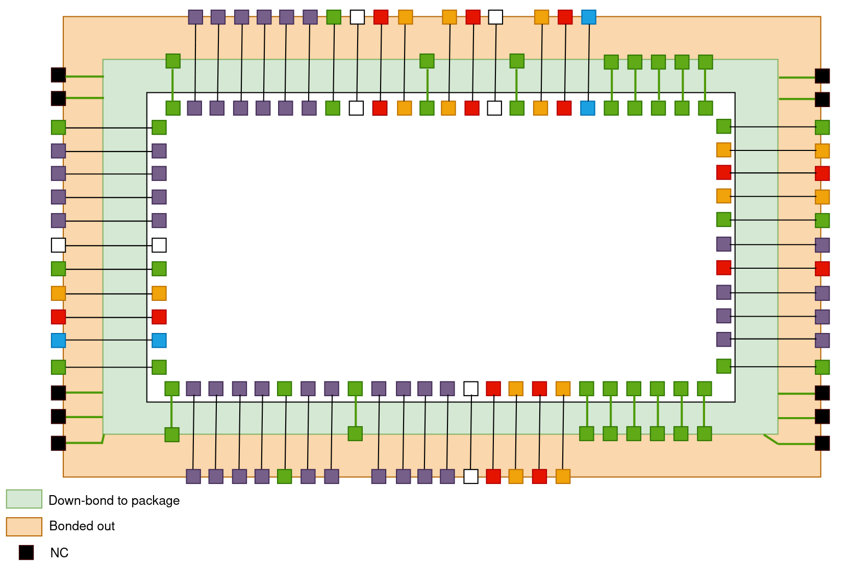
Given that we used a QFN64 package with 16 pins on each side and 64 pins in total, not all pins of the chip were bonded out and some of them were down-bonded to the ground plane. Additionally, some of the package pins were left unconnected. Figure 21 shows how every pin of the chip and the package was connected.
After integrating the I/O cells and the pads, post-layout verification was performed with Cadence Virtuoso. This step required careful analysis of all the DRC & LVS errors to clarify which ones can be waved and which ones needed to be solved. Once this step was completed, the chip was ready for tape-out. The final layout of the chip, including the I/O cells and pads, as viewed in Virtuoso, is displayed in Figure 22.