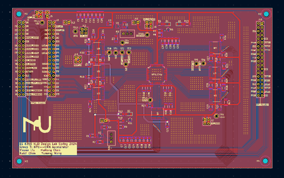
PCB DESIGN
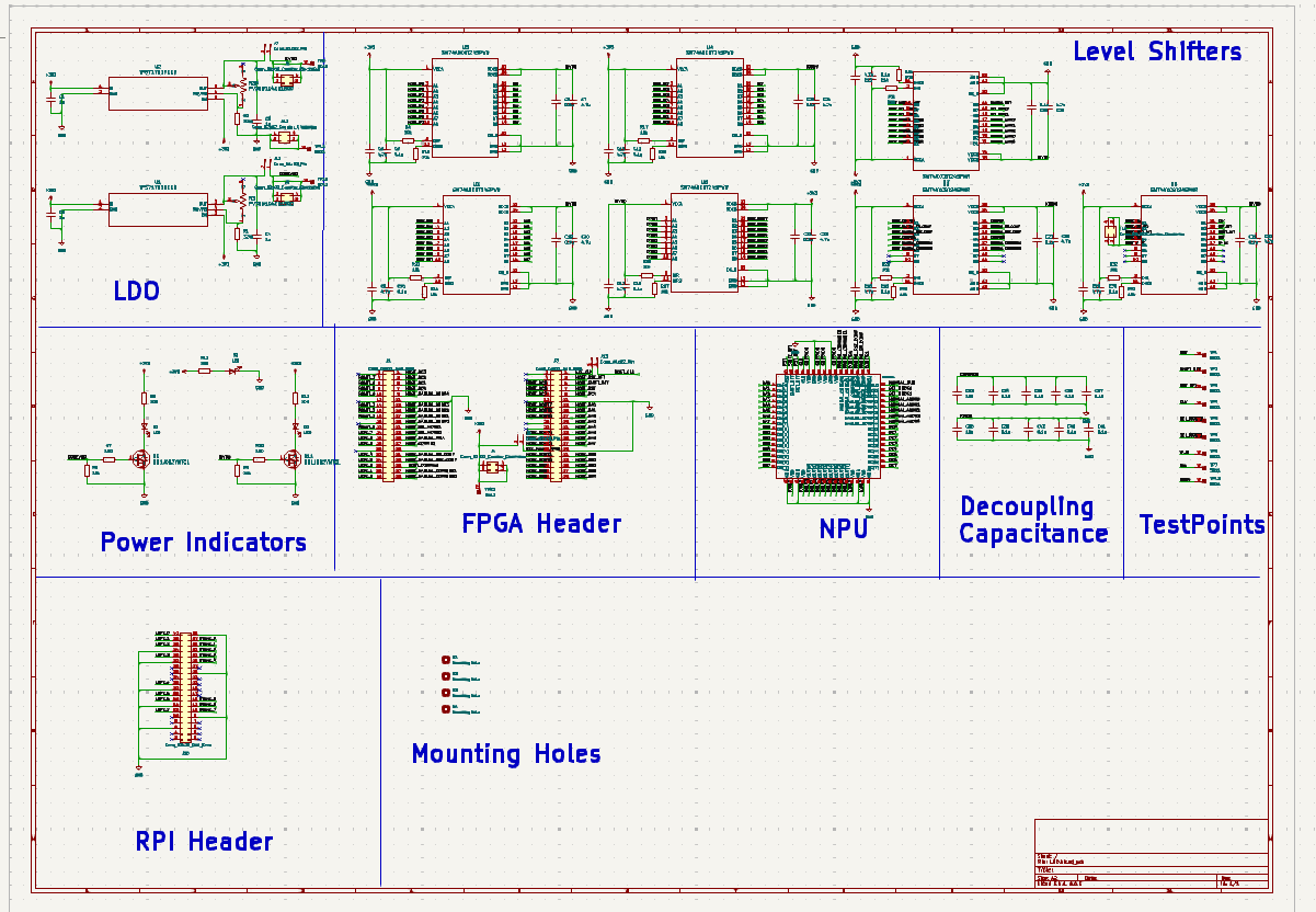
To verify the functionalities of the Neural Processing Unit (NPU), a 2-layer printed circuit board (PCB) was designed using Kicad. The top-level schematic is illustrated in Figure 1. The primary objective of this PCB is to facilitate connectivity with either a Raspberry Pi or an FPGA. As a result, its configuration is intentionally kept simple to ensure efficient communication and testing.
Power Supply
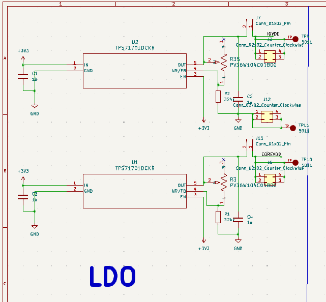
The power for the PCB is supplied either by the RPI IO board or the FPGA, both of which operate at 3.3V. In contrast, the NPU's voltage domains (IO_VDD and CORE_VDD) are both 1V. To generate these 1V outputs, we used two identical LDOs to produce 1V_IO and 1V_CORE, as illustrated in Figure 2. To allow for fine adjustment of the output voltage and to enable overclocking of the NPU when necessary, we replaced one of the feedback resistors with a potentiometer.
LEVEL SHIFTERS
We incorporated six 8-channel level shifters and one 2-channel level shifter to convert input signals from 3.3V to 1V and output signals from 1V to 3.3V, as depicted in Figure 3. All level shifters are bidirectional.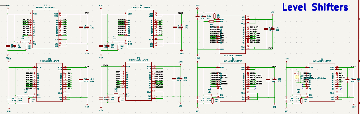
RPI AND FPGA HEADER
Both the Raspberry Pi IO board and the FPGA board feature a series of 2.54mm male headers. To eliminate the need for cables, we designed female headers with matching dimensions, as shown in Figure 6. This design allows for easy connection of the NPU PCB to either the RPI IO board or FPGA board by simply aligning the female and male headers and applying significant force.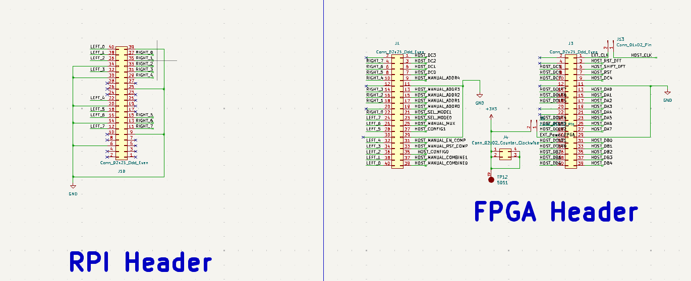
PCB LAYOUT