VERIFICATION
The functionalities were validated using Verilog testbenches and Virtuoso AMS (Analog/Mixed-Signal) simulations. Given that the NPU operates in multiple modes, we developed a comprehensive testbench comprising four tests to ensure that the NPU's computations in each mode precisely matched the results of our MATLAB fixed-point model. The four tests are used for the verification of manual mode, automatic mode, reconfigurable mode, test mode, respectively.
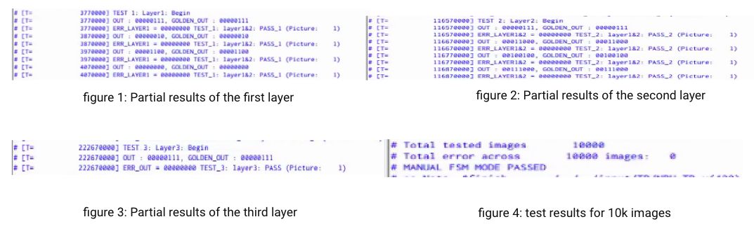
Automatic Mode Verification
In automatic mode, all needed control signals are given from a programmed FSM. The whole FSM contains 3 sub-FSMs to control different layers. The SEL_MODE signal equals to 2'b01.
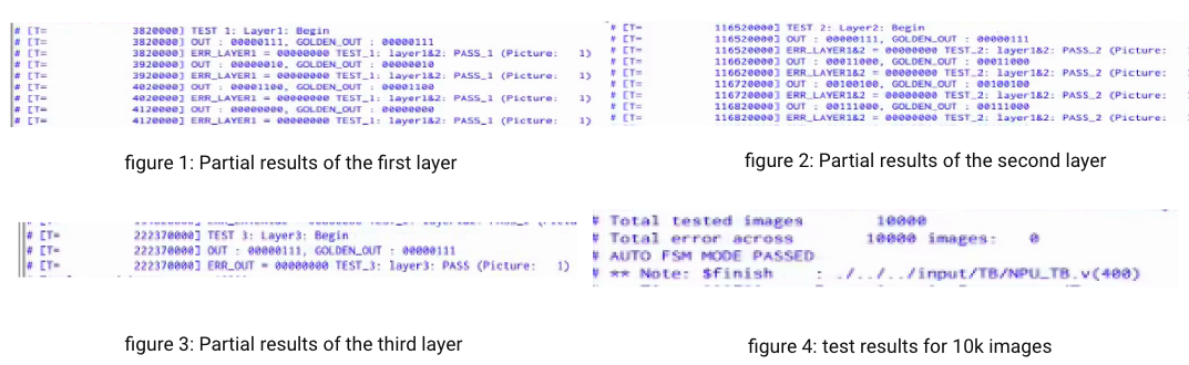
At the beginning, all control signals are provided based on the timing sequence through a testbench, and the Finite State Machine (FSM) is programmed accordingly. To complete a full image verification, three layers must be processed. The first layer is a convolutional layer. After resetting all signals, the process begins by storing weights in the register array. The weights are loaded through a shift register following a specific sequence. Initially, the first three weights of the 4th channel are loaded, followed by the 3rd, 2nd, and 1st channels. As these weights are temporarily stored in the shift register, they are simultaneously loaded into the corresponding positions in the register array. This process is repeated three times, totaling 12 cycles, to store all the weights. The next step is to store the bias values. The method for storing bias is similar to storing weights, but with a simpler approach. A single input pin is used to provide the bias data, which is stored directly in the Bias register. This process takes 4 cycles to complete.
After storing the weights and bias, the chip begins reading and calculating. It can perform three multiplications per cycle. To complete the computation for one kernel, it requires three cycles, plus an additional cycle to add the bias. Next is the ReLU operation. Since there are four channels, it takes four cycles to apply ReLU to the output from the processing element. This timing aligns with the kernel calculation, allowing for a smooth pipeline design. Immediately after one cycle of ReLU, pooling begins. For the pooling process, each comparator must compare four outputs from the ReLU operation, requiring four cycles per channel. With four channels in total, pooling takes 16 cycles. Notably, the first pooling result is available as soon as the 4th en_comp signal is triggered. The total time for the first layer can now be calculated. The first result appears after 33 cycles, consisting of 12 cycles for weights, 4 cycles for bias, 4 cycles for the processing element, 1 cycle for ReLU, and 12 cycles for pooling. Four comparison results from the four channels are produced sequentially. An additional 12-cycle wait is required before the next result. For an 8x8 image, pooling takes 16 cycles per segment, but the last 12 cycles are subtracted from the total as the final result is directly available. The total cycle count for layer 1 is 1045 cycles.
For layer2. It is pretty the same way to calculate the time cycle. One difference is that because we have four figures input, we need 4 times of cycles to store weights. Plus we need 12 cycles to do the convolution plus 1 cycle to add the Bias, total 13 cycles for PE, still 4 cycles for relu, therefore it is 52 cycles for finishing pooling. In addition the input pixels for one figure is 4 times less than that of first layer, So we can calculate the time cycle for second layer. 48+4+13+1+48=114. when it comes to the pooling part of second layer, it is a 4 by 4 figure, one for 52 cycles, and we can subtract last 48 cycles for last result. The total cycle for layer2 is 898.
For layer3. It is way easier than last two layers, we just need 22 cycles to store four 4 by 4 pixels, 1 cycle to store bias, another 22 cycles to do the convolution plus one cycle add bias, 1cycle for getting the index and repeat 10 times to get the final results. Then we can calculate the total is 22+25*10 = 272.
Figure 2 shows the test result of auto mode. All simulation passed.
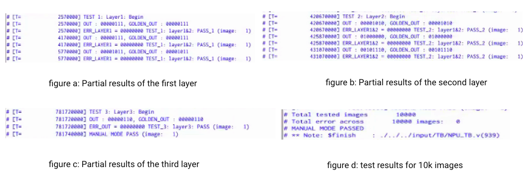
Manual Mode Verification
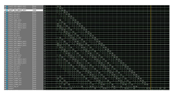
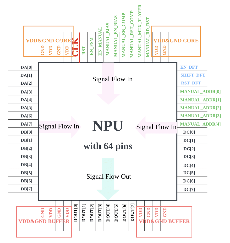
In manual mode, all required control signals are highlighted in green in Figure 1. The 'SEL_MODE' signal is set to 2'b00. Due to the limitation of pins on the chip, it is not possible to provide all the necessary signals for each of the four Processing Elements (PEs) simultaneously. To address this constraint, only one PE is used for computation in manual mode, rather than all four PEs operating together. As a result, the computation time is significantly longer. Processing a single image requires a total of 5818 cycles.
Figure 3 shows the test result of manual mode. All simulation passed.
Reconfigurable Mode Verification
In reconfigurable mode, the SEL_MODE signal equals to 2'b11, and we ues SEL_CONFIG signal to activiate the specific FSM control of assigned layer. It totally costs 2196 cycles for 1 image.
Figure 4 shows the test result of reconfigurable mode. All simulation passed.
Test Mode Verification
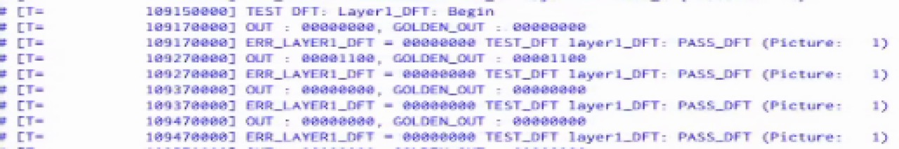
In test mode, the 'SEL_MODE' signal is set to 2'b10. During debugging, no computation takes place. The process begins with verifying the functionality of the test registers. Initially, a reset (rst) is performed, followed by enabling the Design for Testability (DFT) signal and the shift signal. The test registers operate as a shift register, allowing a sequence to be scanned in. After waiting for 42 cycles, the output is checked to ensure it matches the input sequence. The next step is to verify the correct functioning of the sequential circuit. This is achieved by loading the data from each sampled register into the test registers. Subsequently, over the next 42 cycles, the data from each register is shifted out, enabling an assessment of the sequential circuit's behavior.
To facilitate debugging, an 'enable' signal can be asserted at any cycle as needed. When this signal is raised, computation in other parts of the chip is temporarily halted. Once halted, the system follows a predefined timing sequence to sample data at all points of interest. This mechanism ensures that the internal state of the chip is captured at specific moments for later analysis. After sampling, the captured data can be shifted out one sample at a time, allowing for a detailed examination of the chip's internal state. This process provides engineers with the ability to review and debug system behavior in a controlled manner. Once debugging is complete, deasserting the 'enable' signal allows the chip to resume computation from the point where it was halted. Importantly, no data is lost during this process, as the system is designed to preserve its internal state. By maintaining proper data input timing, the chip can seamlessly continue its operations without disruption. This approach provides a non-destructive method for debugging, ensuring continuity of computation while enabling in-depth analysis.
Figure 5 and 6 shows the test result of test mode. All simulation passed.