
DEMO2
Demo2 is primarily used in the early stages to verify the accuracy of the chip after tape-out and to evaluate the maximum speed achievable by the chip. An FPGA is connected to a PCB for this purpose. Two main tests were conducted:
1. Accuracy Test
Data from the dataset and theoretical intermediate values are stored in the FPGA's RAM. The FPGA sends control signals and input data to the chip, initiating its operation. Once the chip starts working, the FPGA captures each output from the chip and compares it with the stored intermediate values to ensure the chip's accuracy. Essentially, this involves reprogramming the previous testbench into synthesizable RTL code.
2. Performance Test (the base of Demo1)
The FPGA stores only the pixel data of the images and the trained weights, which are sent to the chip along with control signals to start its operation. Subsequently, the FPGA receives the chip's intermediate outputs, reorganizes and stores them in RAM, and feeds them back to the chip. Finally, the FPGA captures the chip's final output, which is the chip's prediction result. The FPGA converts this output to decimal format and displays it on a digital display. Our maximum frequency is 18 MHz, whereas the target frequency during chip synthesis was 100 MHz. We investigated the reasons for not achieving 100 MHz, identifying two primary factors:
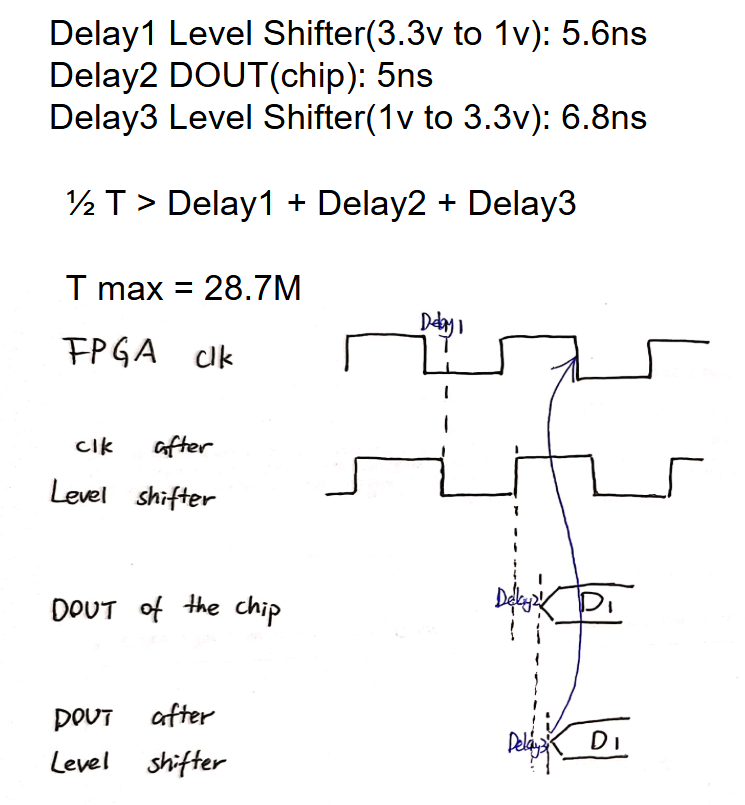
1. Level Shifter and DOUT Delays
The delays in the Level Shifter of the input/output section and the DOUT of the chip itself contribute significantly. For the FPGA to correctly capture the chip's output, there is an inherent theoretical maximum frequency. The detailed derivation process is shown in Figure 1. By measuring the delay of the Level Shifter on the PCB, we calculated the theoretical maximum frequency to be 28.7 MHz.
2. IOVDD Jitter
Using an oscilloscope, we observed significant jitter in the IOVDD, as shown in Figure 2. This jitter further reduces the maximum achievable frequency below the theoretical value.