CUSTOM CIRCUITS
In addition to the NPU core, we have designed three types of circuits in this project: an input buffer to drive the NPU core, an output buffer to drive external circuits, and a Schmitt trigger to process clock signals.
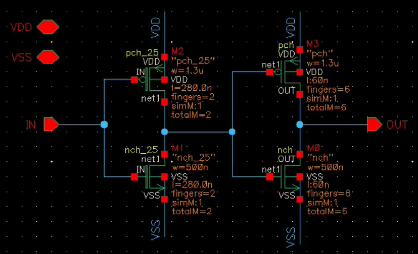
Input Buffer
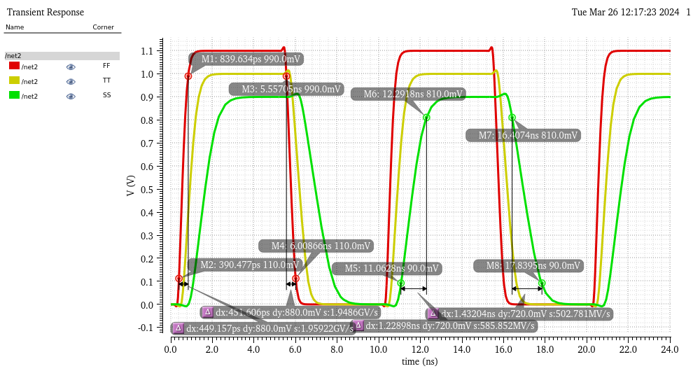
The input buffer features a two-stage design optimized for performance and protection. The first stage uses 2.5V thick oxide devices to provide enhanced Electrostatic Discharge (ESD) protection, while the second stage employs 1V thin oxide devices for faster switching and lower power consumption. Designed to drive a 1pF load, the buffer achieves balanced rising and falling times with a PMOS/NMOS width ratio of 2.6/1. Simulation across process-voltage-temperature (PVT) corners reveals rise times of 449ps (ff), 448ps (tt), and 1.23ns (ss), and fall times of 452ps (ff), 478ps (tt), and 1.43ns (ss). Thick oxide devices interface with the pad, while thin oxide devices connect to the NPU core.
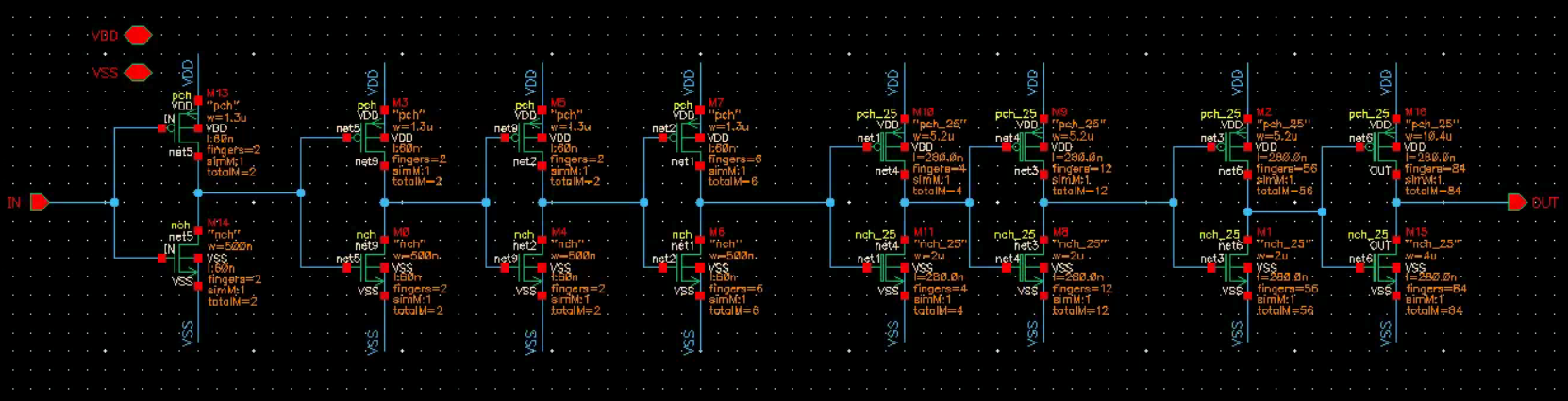
Output Buffer
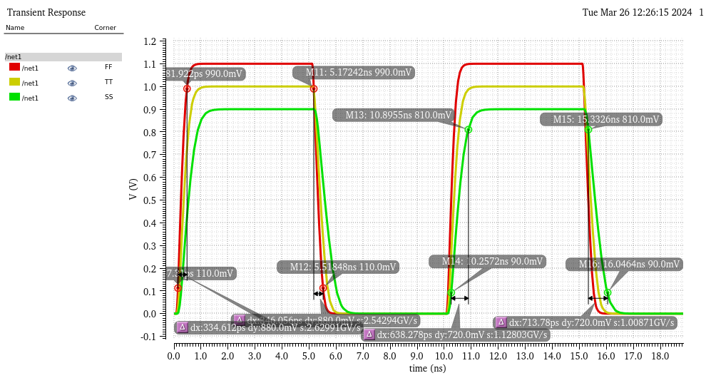
The output buffer consists of eight stages and maintains a PMOS/NMOS width ratio of 2.6/1, similar to the input buffer. The first four stages use 1V thin oxide devices for faster switching and reduced capacitance, while the subsequent stages use 2.5V thick oxide devices for robustness and ESD protection. Each stage is scaled to be approximately three times larger than the previous one, enabling the buffer to efficiently drive a 10pF load. Simulations across process-voltage-temperature (PVT) corners show rise times of 335ps (ff), 721ps (tt), and 638ps (ss), and fall times of 346ps (ff), 769ps (tt), and 714ps (ss). The thin oxide devices interface with the NPU core, while the thick oxide devices connect to the pad.
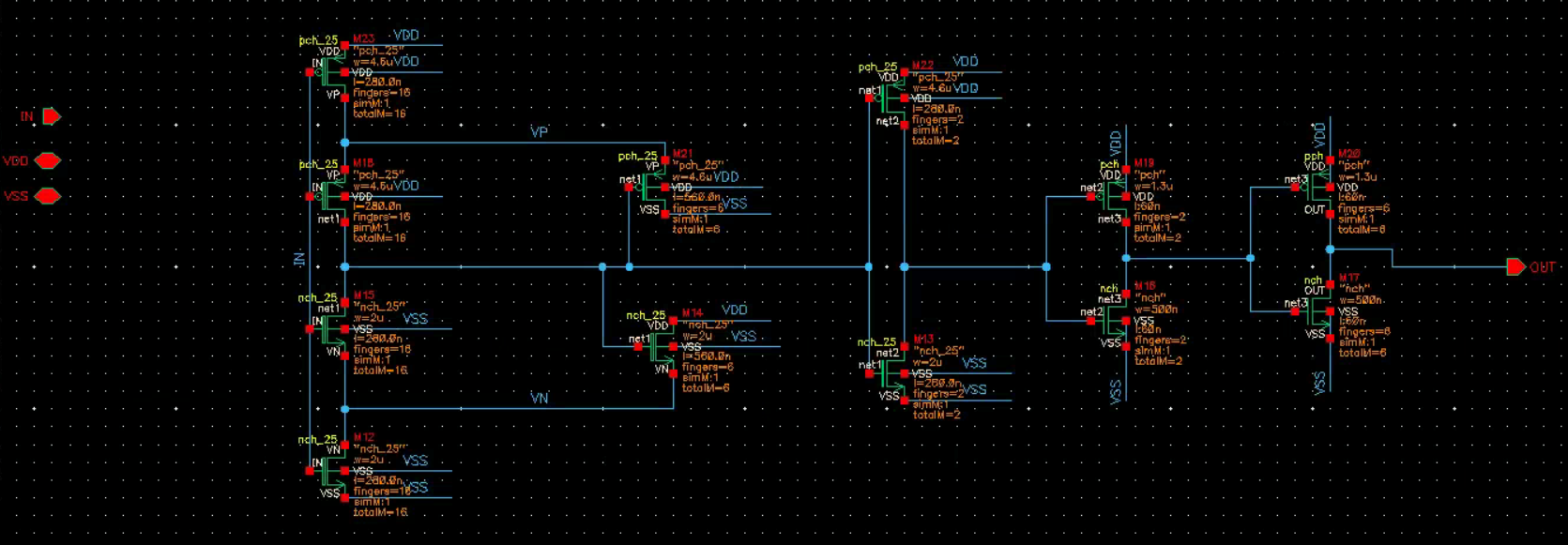
Schmitt Trigger
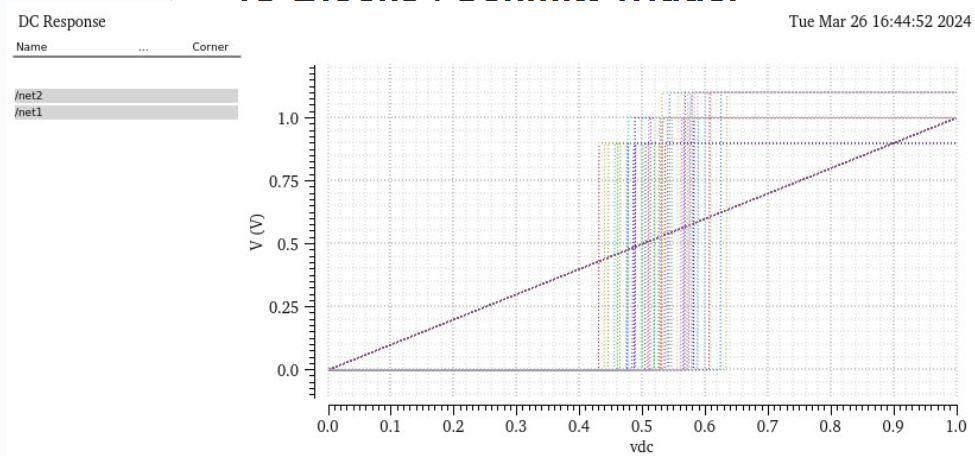
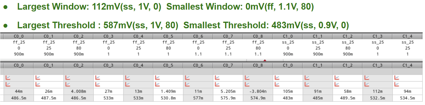
The Schmitt trigger is designed to improve clock signal quality and stability by leveraging hysteresis, which defines distinct rising and falling thresholds to suppress noise-induced switching. This ensures clear, steep clock edges, enhancing reliability and precision in digital circuits. Constructed using 2.5V thick-oxide devices, the Schmitt trigger interfaces with the CLK pin. Simulations across PVT corners reveal a largest hysteresis window of 112mV (ss, 1V, 0deg C) and a smallest window of 0mV (ff, 1.1V, 80deg C). The threshold voltage ranges from a maximum of 587mV (ss, 1V, 80deg C) to a minimum of 483mV (ss, 0.9V, 0deg C), ensuring robust performance under varying conditions.