LAYOUT
Figure 1 shows the layout of the NPU chip, with the NPU core centrally placed and generated using TCL scripts provided by Rui Xu in conjunction with Cadence Innovus. The input buffers are located near the input pins, the output buffers next to the output pins, and the Schmitt trigger close to the clock pin to optimize signal integrity and timing. The whole design integrates auto PNR for the core, along with a padframe, decoupling capacitors (52pF for VDD_core and 177pF for VDD_bf), and metal fill to ensure electrical stability and performance.
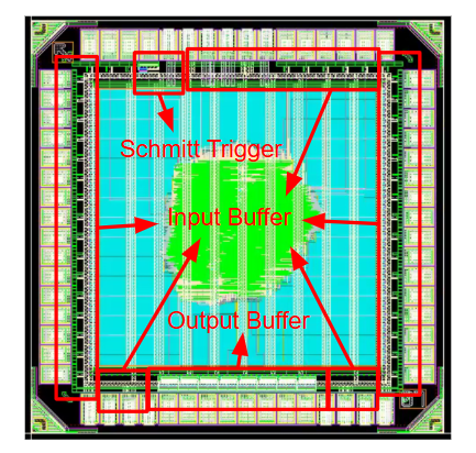
Figure 2 provides a detailed view of the digital core layout, which measures 800 x 800 with a total core area of 0.555 mm2. The core density is 16.77%, and the core utilization is 22.43%. The power ring is implemented using M8 and M9 metal layers, with M8 used for power stripes. All pins are placed on the M4 layer for connectivity.
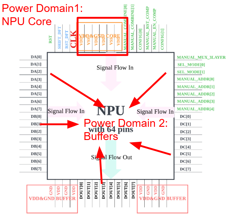
Figure 3 depicts the floor plan of the NPU chip, which features two 1V voltage domains. The CORE_VDD domain, with four grouped pins, powers the digital core, while the IO_VDD domain, also with four pins, supplies power to all IO buffers, the Schmitt trigger, and their ESD protection circuits. The IO_VDD pins are symmetrically divided into two groups at opposite corners of the layout to balance power distribution and minimize interference or signal integrity issues. Additionally, the design includes six GND pins to ensure stable grounding.