Once the photocurrent is generated by the sensor board, it is AC coupled and fed into the single ended transimpedance amplifier (TIA). This is the only single ended stage in the signal chain due to the input current being single-ended. The TIA performs three functions at this stage:
Convert the current signal to a voltage.
Contribute to the gain stages by amplifying the signal.
Bias the output at 500mV
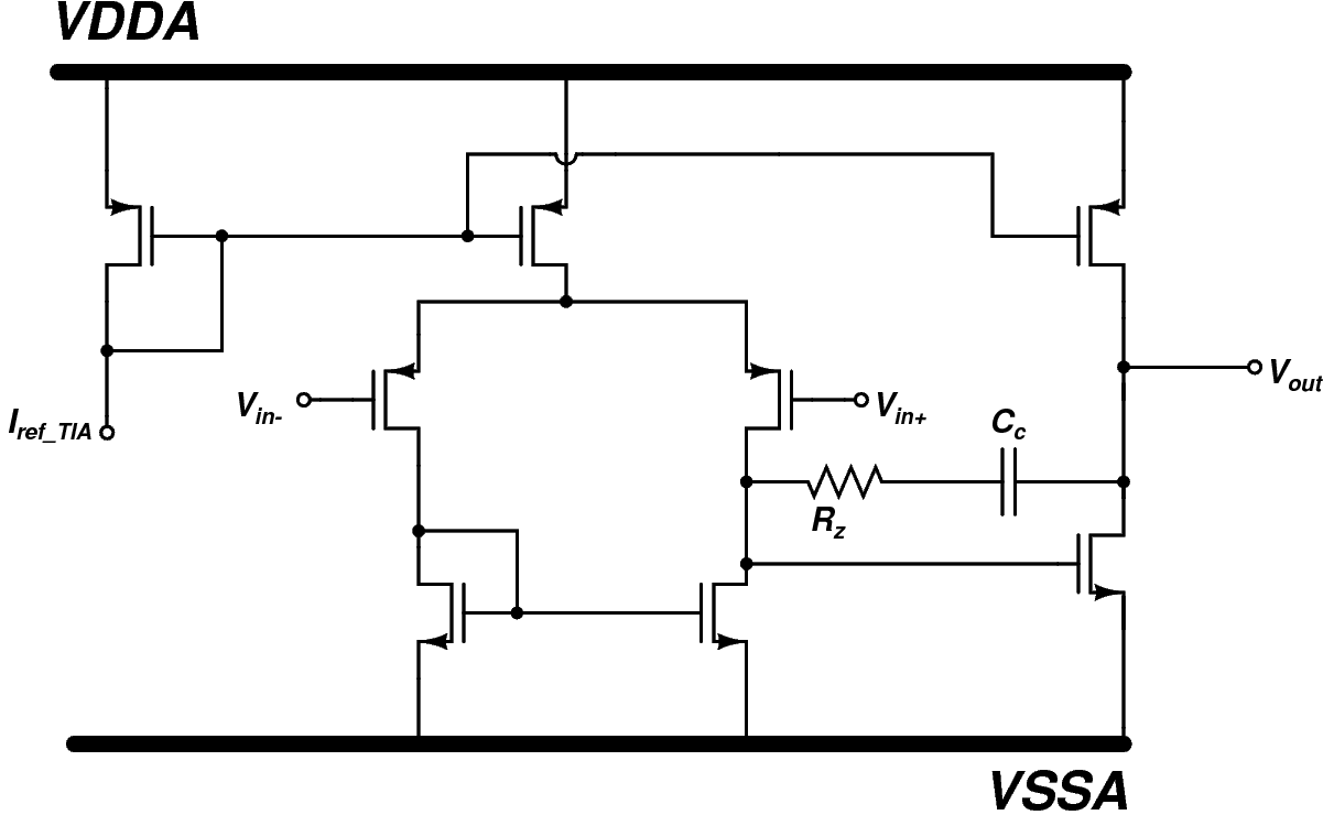
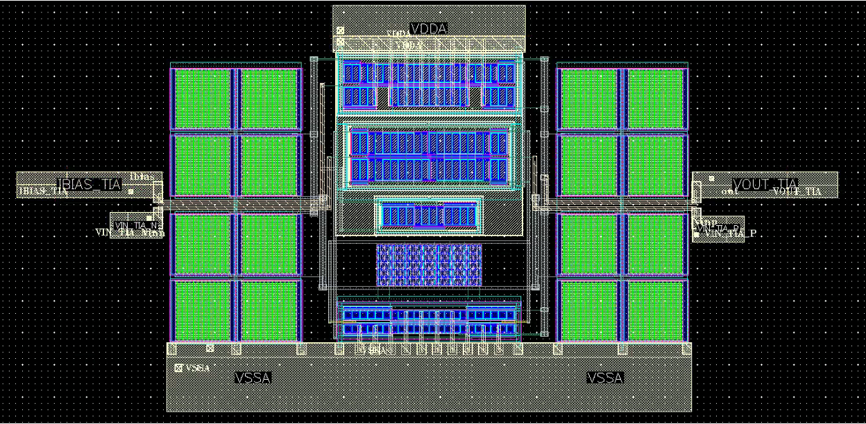
The TIA structure consists of an OTA (basic architecture shown in Fig.1 and 3) with RC feedback as shown in Fig.2. In order to bias the output at 500mV a reference voltage is input at the positive terminal of the OTA.
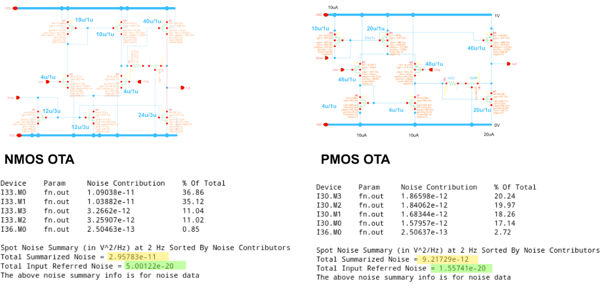
The TIA utilizes a classical two stage miller compensated OTA (Fig.3) with a PMOS input pair. Since the photocurrent signals that would be input into the TIA are highly susceptible to noise (particularly due to their small amplitudes), a TIA with minimal input and output noise had been the ideal choice. Noise analysis was run for each for NMOS and PMOS input pair OTAs sized for similar gain and phase specifications. The noise analysis results favoured a PMOS input pair, as observed from Fig. 2 and 3.
Fig.2 - Parametrized Noise Analysis
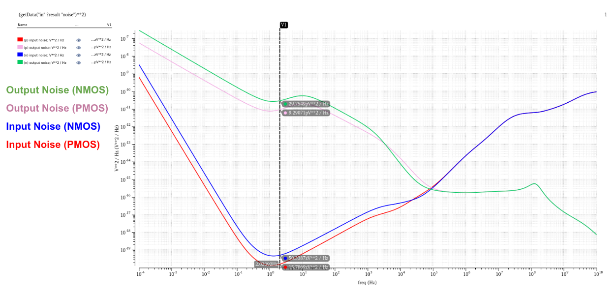
Fig.3 - Input and Output noise waveforms across frequencies. Noise values were taken from typical heart rate frequency of ~1Hz.
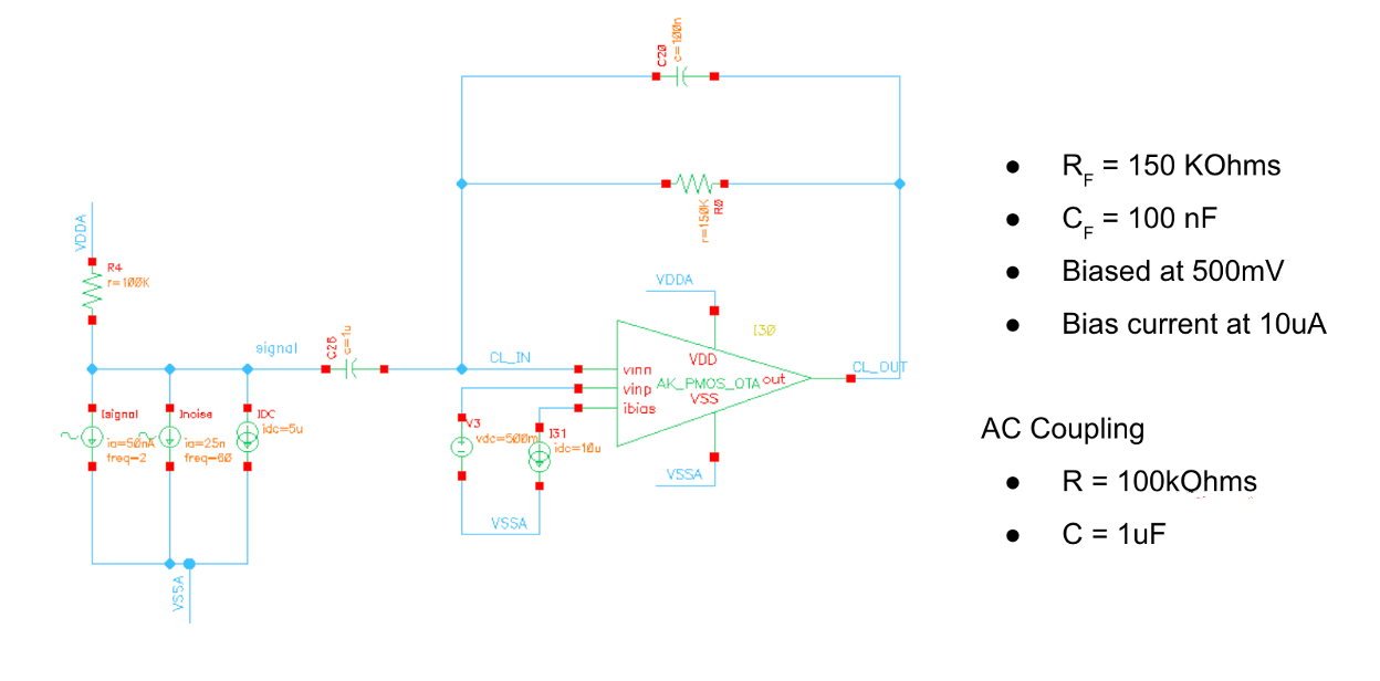
The testbench for the TIA is shown below.
Fig.4 - TIA Testbench with input signal parameters
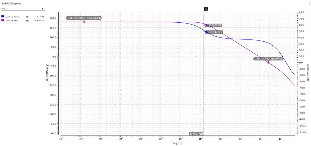
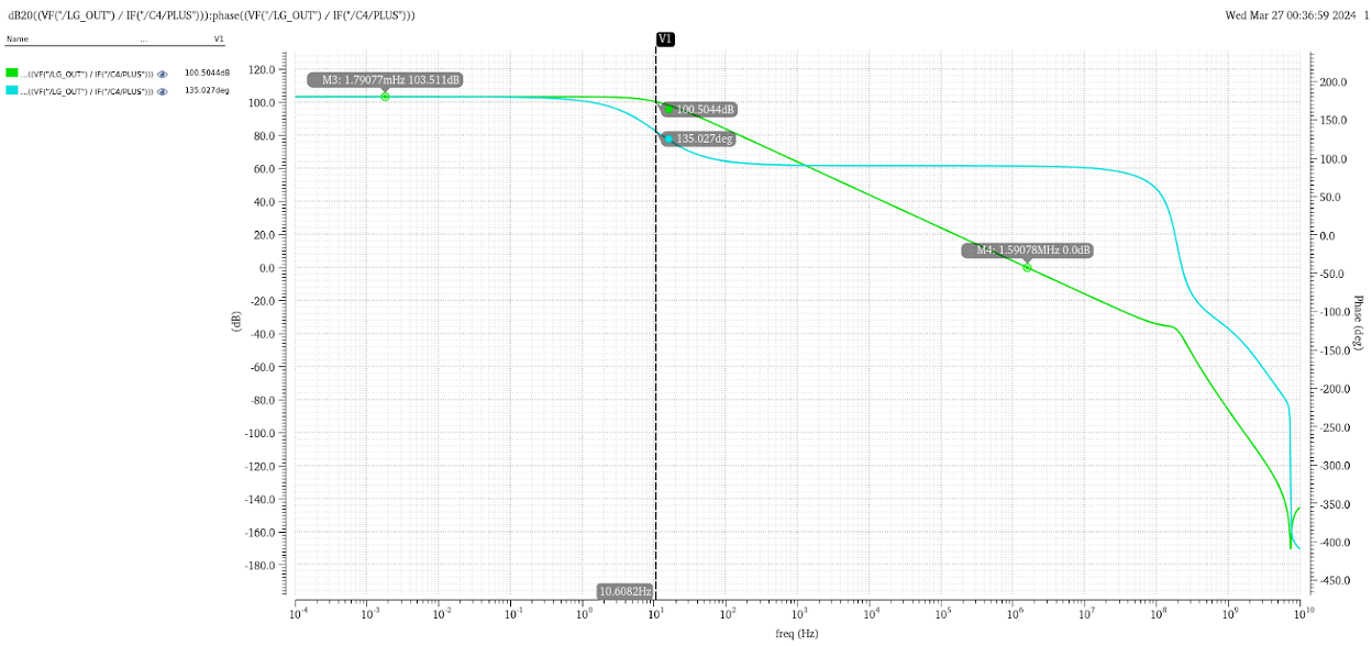
The TIA Open Loop, Loop Gain and Closed Loop results are shown below.
Fig.5 - TIA Open loop Gain Frequency Analysis (64.5dBOhm, 15kHz 3dB frequency)
Fig.6 - TIA Loop Gain Frequency Analysis (103.51dBOhm, 10.61Hz)
Sufficiently separated poles were targeted for a higher phase margin. The low frequency input (0.2-0.4Hz for breathing rate and 0.6-4Hz for heart rate) allowed a lower first pole that was still far away enough from the desired frequency range. As seen in Fig.6 the dominant pole sits at 10.61Hz, resulting in a sufficient phase margin of ~90 degrees.
Fig.7 - Closed Loop Frequency Analysis (103.5dBOhm, 10.8Hz)
The closed loop gain had been as expected at 103.5dBOhm for 150k feedback, with the dominant pole at 10.8Hz.
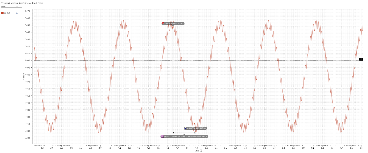
Fig.7 - TIA Output Transient
The output of the TIA had been verified to be as expected from an input signal that based on the testbench described in Fig.2 after AC coupling (2Hz signal with 50nA amplitude, 60Hz signal with 25nA amplitude, 5uA DC).
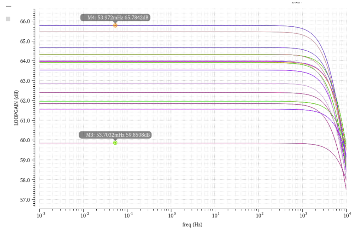
PVT was run across corners to determine the best and worst performing corners. Based on the above figures these corners were determined to have been from the ff corner 100°C 1.1V and the best forming at ss corner 0°C 0.9V. The closed loop PVT did observe a very low variation of gain across corners.