PCB Design
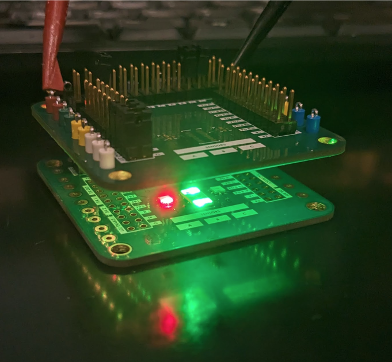
We sincerely thank our TA, Alfred Festus Davidson for providing us with the optical sensor board, which has been the primary input block for our measurements and demonstration.
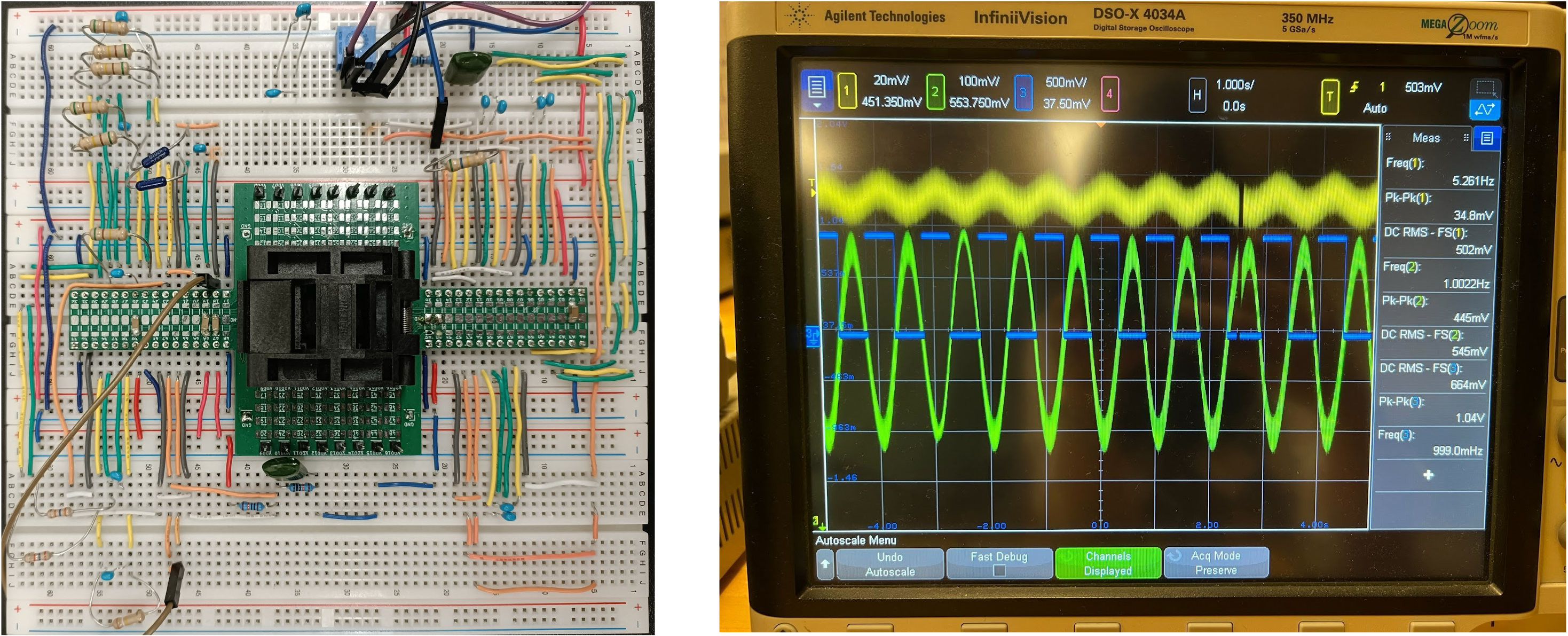
An initial phase of measurements was conducted using a breadboard as shown in the figure below.
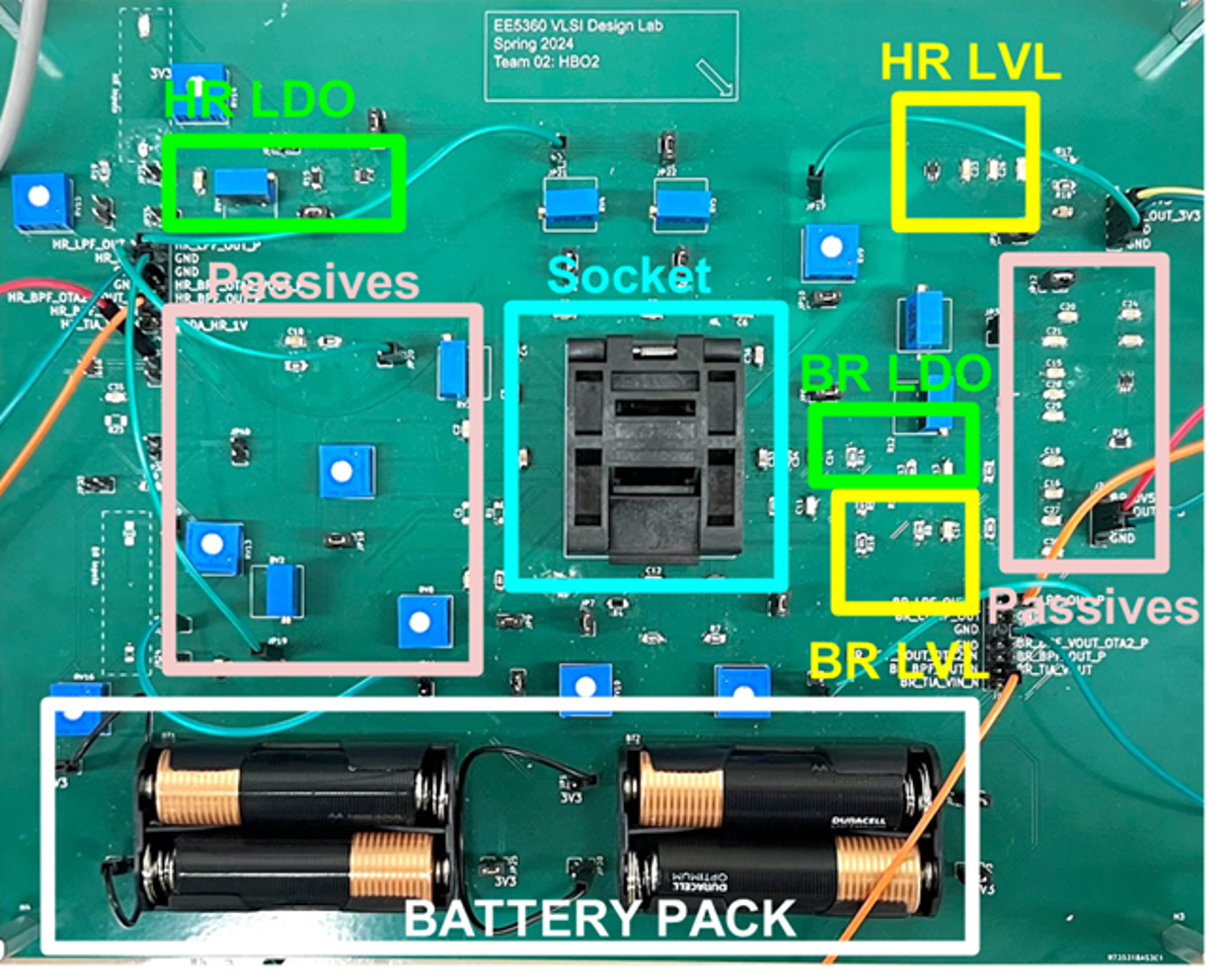
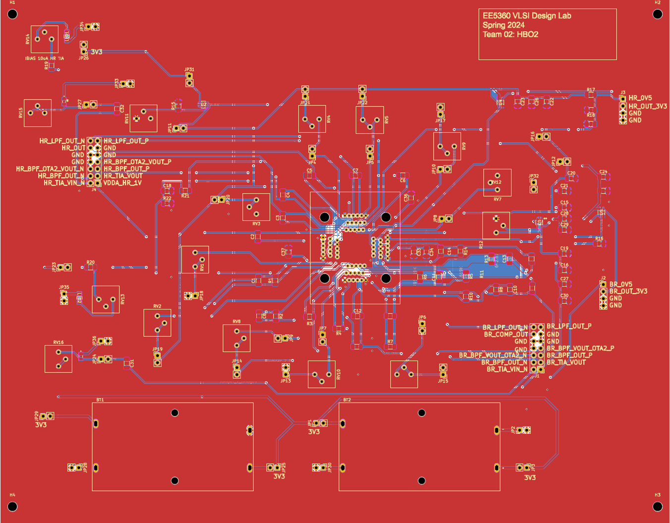
- Main Socket - a socket was soldered onto the PCB to facilitate the mounting and connection of the chip to the external active and passive components.
- Resistors and Capacitors - the passives provided on the PCB are of three types.
- Resistors - these serve as feedback elements in the breathing rate path and voltage dividers in LDOs and reference generators.
- Capacitors - these serve as feedback elements in the heart-rate and breathing-rate path and decoupling capacitors for supplies and references.
- Potentiometers - these help generate bias currents for circuit blocks on the chip.