A fully-differential amplifier (FDA) was designed and characterized to be used in the filtering stages following the Trans-impedance Amplifier (TIA). This FDA follows a traditional two-stage miller compensated Operational Transconductance Amplifier (OTA) architecture.
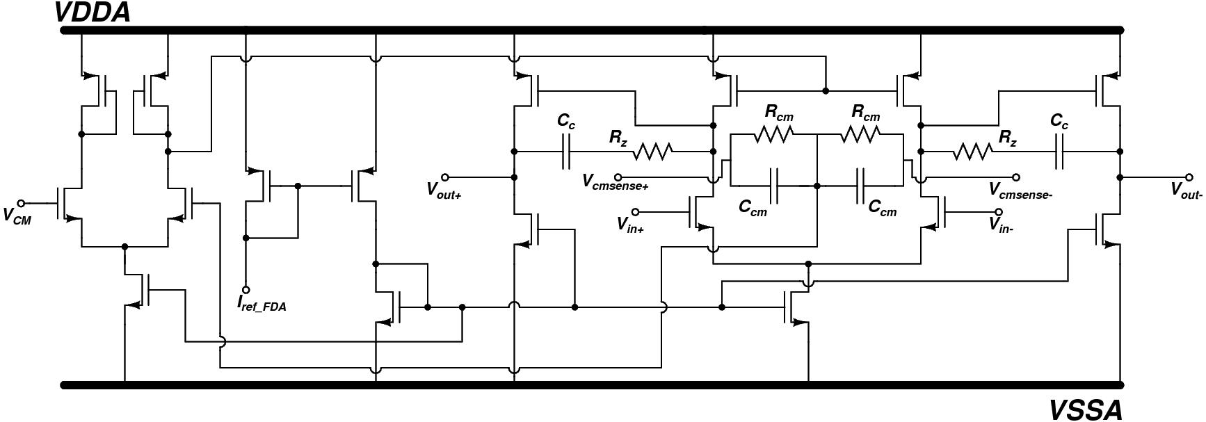
As mentioned, this architecture has two separate gain stages that are cascaded in-order to achieve a two-stage architecture for higher gain. The first stage is a common differential pair that consists of a current source and two sets of NMOS and PMOS transistors. The inputs (Vin+ and Vin-) are compared at the gates of the NMOS transistors (design choice) and the outputs are taken from the drains of NMOS & PMOS transistors and fed to the next stage.
Designing a two-stage amplifier necessitates the inclusion of another amplifier stage, namely the common-mode feedback amplifier (CMFBA). Such an amplifier helps in further rejecting the common-mode signals - a feature that’s already inherent to a differential architecture - and also helps in setting the DC bias of the output signals (Vout+ and Vout-) coming from the second stage.
The designed CMFBA largely operates under the same principles followed by a differential pair. In this particular amplifier, one of the differential inputs is an external voltage source that sets the desired output operating point, whereas the other end stems from a RC network that is designed on chip. This particular RC network consists of resistors and capacitors connected in series and parallel fashion, and the respective input terminals for this network are dubbed as Vcmsense+ and Vcmsense-. While these nodes (Vcmsense+ and Vcmsense-) are shorted to Vout+ and Vout-, respectively at the top level, these nodes are left floating at the testbench level to help probe the gain of the corresponding CMFBA.
The output of CMFBA is then connected to the PMOS transistors in the 1st stage to complete the feedback loop. The reference voltage to the CMFBA is chosen to be 500mV as a design choice made at the system level. Thus, the CMFBA ensures that the voltage at the output of the second stage is at 500mV.
The current source for this FDA is PMOS in nature compared to the other current sources on this chip. An external bias voltage is applied to the drain of a gate connected PMOS transistor, whose voltage is then used to drive 10uA of current into the main amplifier block. This concludes the design description of the FDA, the following section describes the simulation and layout for this particular FDA.
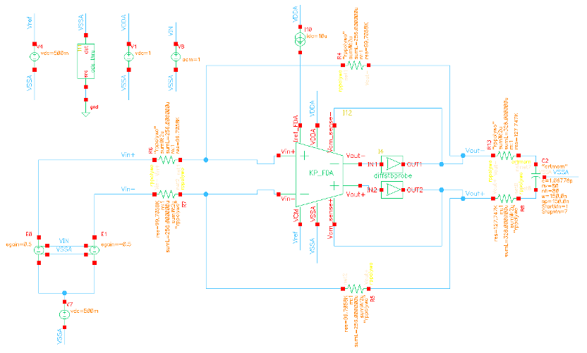
Fig.2 - FDA Testbench
The figure above shows the testbench using which the FDA was simulated. CMFBA has 4 terminals which can probed at the testbench level using diffstbprobe element in cadence. The FDA is placed in a unity gain feedback setting to measure its gain accurately. An appropriate RC load is placed at the output to ensure its being simulated in a desired environment of operation.
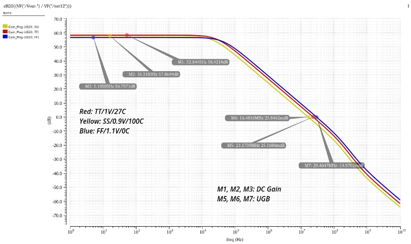
Fig.3 - FDA Open Loop Gain (PVT)
Fig.4 - Calculated Gain values across PVT
The above figure and table depict the simulated gain response for the FDA across different process corners. This FDA was designed to have a gain of 60dB and the gain is within 3-4dB across process corners. UGB for this particular amplifier is largely relevant as the frequencies at the system level are around 0.2-4Hz. This FDA was overdesigned - thanks to the advanced modern devices available in the design technology - as far as UGB is concerned. Any gain beyond 40dB would be sufficient for the filters to do their job including the FDA in their architecture, and in that regard, the gain was pushed to 60dB keeping sizing constraints in mind.
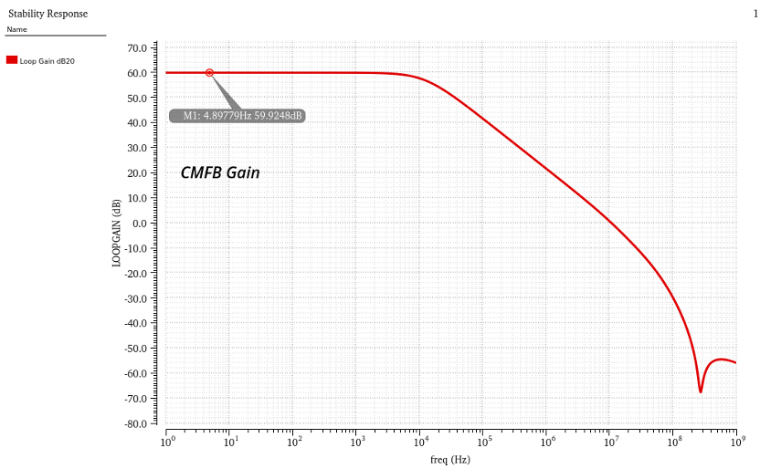
Fig.5 - CMFB AC Response
The above figure shows the simulated loop gain response of the CMFBA. This response indicates that the CMFBA will ensure common-mode signals are rejected, and also function to provide the required DC bias at the output of the 2nd stage in the FDA. Similar to the FDA, this amplifier is overdesigned as far as the UGB specification is concerned.
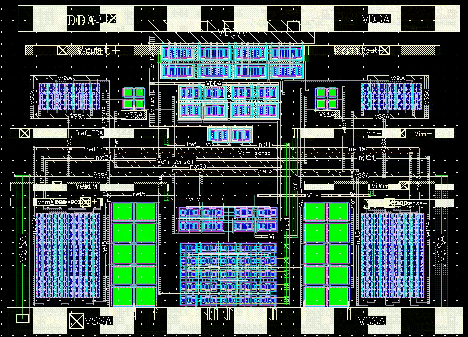
Fig.6 - FDA Layout
The image above shows the layout of the fully-differential amplifier. Thick metal strips are placed on the top and bottom to make the connections to supply and ground easier at the top-cell level. The transistors near the supply strip are PMOS and the transistors near the ground are NMOS. Dummy fingers and devices were used for all transistors to help mitigate process variations. The common-mode resistors are placed on either side of the NMOS transistor bunch, with resistors alternating on either side to maintain symmetry. In a similar vein, common centroid matching was used for laying out both PMOS and NMOS stacks to help deal with mismatch which is a key aspect to aware of when designing analog circuits. The miller compensation capacitors were placed on either side of the NMOS stacks whereas the common-mode capacitors were placed on the either side of the PMOS stacks.
Multiple such copies of the same FDA were used for designing all filter stages across both HR and BR paths. This concludes the simulation and layout details of the FDA.