After the signal goes through the amplification and filtering stages (Transimpedance Amplifier & Biquadratic Filter), the differential output is then fed to a comparator. The comparator is a fully differential structure and makes use of the following current steering architecture. The main advantages of using a comparator are -
The comparator sets the power threshold for the output signal. It converts the periodic input waveform into a square wave (digital signal), which is the level-shifted (externally) and sent to the Arduino, which counts the edges to determine the frequency.
The comparator provides hysteresis - any spurious changes in the input signals can be eliminated as long as they are within the hysteresis window.
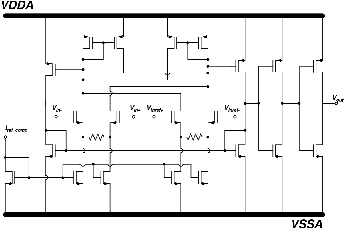
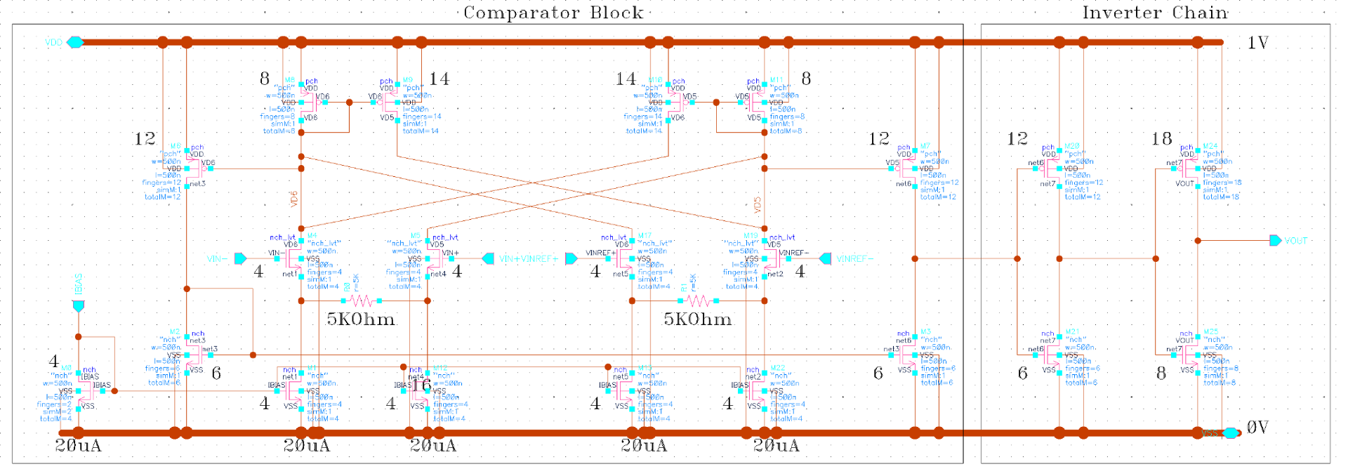
The comparator takes in 4 inputs - two differential AC input signals and 2 reference inputs. The output produced is a square wave the swings between 0 and 1V. The comparator is biased using a 20uA DC Current source. The comparator achieves hysteresis through the positive feedback mechanism that is realised using the cross-coupled PMOS current mirrors. The schematic of the comparator is shown below.
Fig.3 - Comparator Schematic
The hysteresis width of the comparator is determined by the following factors -
The ratio of sizes of the PMOS transistors in the cross-coupled current mirror.
The gm/id (or overdrive voltage) of the transistors.
Some more features of the architecture shown are as follows -
LVT devices have been used at the inputs to ensure that the current mirror foot is in strong inversion.
Second stage design accomplishes differential-to-single ended conversion.
Source degeneration resistances used in the NMOS input pairs for improved linear input range.
Comparator output is sent to a buffer to improve the rise and fall slopes of the output square waveform.
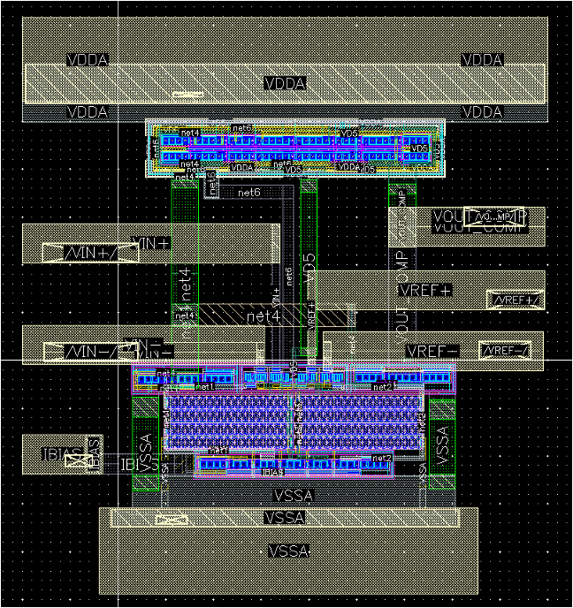
To ensure good layout practises, a baseline width and length have been defined for the transistors and their transconductance is modified by changing their finger width. Being a differential circuit, the comparator has been laid out symmetrically. The layout of the comparator has been shown below.
Fig.2 - Comparator Layout
Dummies have been provided for all transistors in the main comparator block that ensure mismatch errors are minimal in the transistors. Since all pins for the comparator are accessible at the chip level, guard rings have been provided for critical transistors in the block, which help in shielding the devices from ESD.
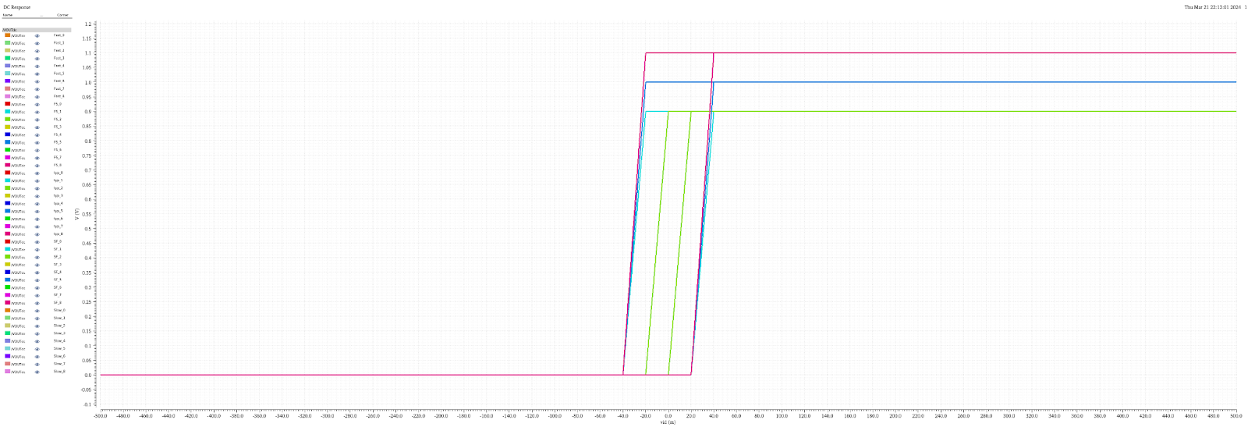
The comparator performance has been evaluated using DC and Transient simulations. The test bench has been created as follows, with a loading of 10pF to mimic the worst case output loading. A DC sweep has been carried out to obtain the hysteresis voltage range. The DC Sweep Analysis(across PVT) for the Comparator is shown below. The typical hysteresis voltage is about 60mV.
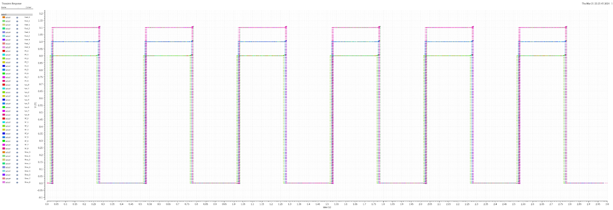
The transient simulation for the comparator is shown below. The rise and fall slopes of the comparator are at around 100-300ns, which is sufficiently fast for the frequency of operation (0.2 to 4 Hz).