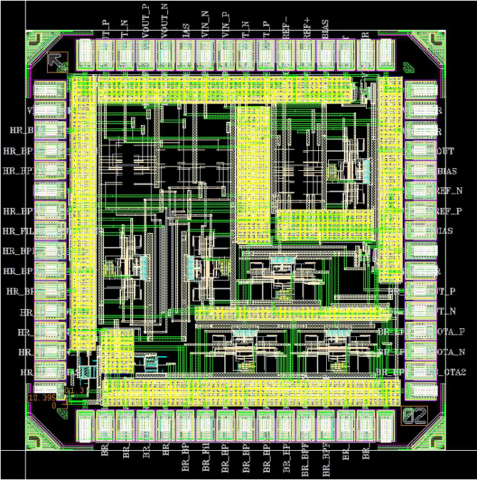
IC Design

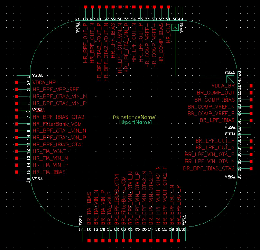
The top level of the PPG IC has 64 pins. The top level symbol of the chip is shown below. The pins associated with HR signals are placed at the top & left side of the chip, and the pins associated with the BR signals are placed at the bottom and right side of the chip.

Chip Symbol
Fig.1 - Top Cell Symbol
The top level symbol of the chip is shown below. The pins associated with HR signals are placed at the top & left side of the chip, and the pins associated with the BR signals are placed at the bottom and right side of the chip.
HR Schematic
Fig.2 - HR Top Level Schematic
BR Schematic
Fig.3 - BR Top Level Schematic
The chip was designed to have separate power domains for the heart rate path and the breathing rate path. The breaks on the supply rail on the bottom left and top right of the above Top-Chip schematic represent these distinct domains.
Chip Schematic with Bondwires and Bondpads
Fig.4 - Chip Schematic with Bondwires and Bondpads
Since the power domains are distinct and the pin orientation aligns with the break in the power rails, the individual components have been laid out in order to optimize wire lengths. To ensure that the heart rate and breathing rate blocks are close to their respective power domains (as discussed above), each block is physically located and routed on the upper left (for HR) or the bottom right (for BR). This distinction is more clearly illustrated below. Guard rings have been placed for all devices with outputs being brought up outside the chip. Dummies for matching-critical devices have been provided to minimize mismatch related offset effects. Images for the chip-level layout and floorplan have been provided below.
Floorplan of the Chip
Fig.5 - Floorplan of the Chip
Layout of the Chip
Fig.6 - Layout of the Chip


Back to top