While there are multiple ways in which bandpass and lowpass filters can be designed, there are few toplologies that take advantage of a differential architecture and by considering block-size, ease of implementation and specifications, Tow-Thomas Biquad based Bandpass and Lowpass Filters were designed for the amplification/filtering stage in our chip.
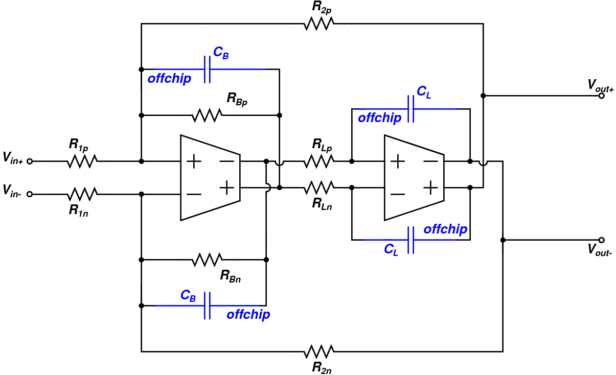
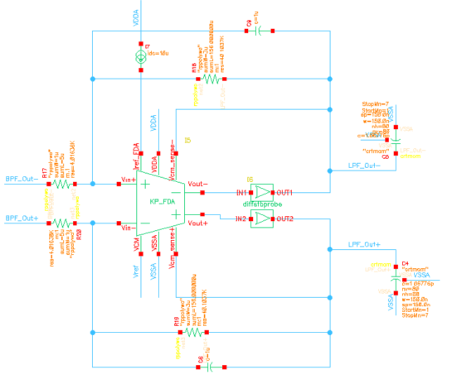
Tow-Thomas Biquad based BPF's schematic is shown in the image above. This architecture uses FDA's designed earlier as OTA's and sets a bandpass region based on the values of the passives. Considering the frequency range in which breathing rate and heart rate can be detected, the capacitors were implemented off-chip given the size constraints of the final chip. Thus, this BPF was designed assuming an off-chip capacitance of 1uF.
Fig.1 - BPF Schematic
Appropriate resistance values were chosen to set the passband sections for BR and HR, and given that BR frequency range is an order of magnitude lower than HR, all respective resistors for BR were implemented off-chip. However, for the HR path, all resistors were implemented on-chip given the resistor values were feasible to be laid out on-chip.
The range of frequencies for HR and BR are 0.6 - 4 Hz and 0.2 - 0.4Hz respectively, and the values of passives and the gain obtained for each path through this BPF is outlined in the tables included below.
Fig.2 - BPF Testbench
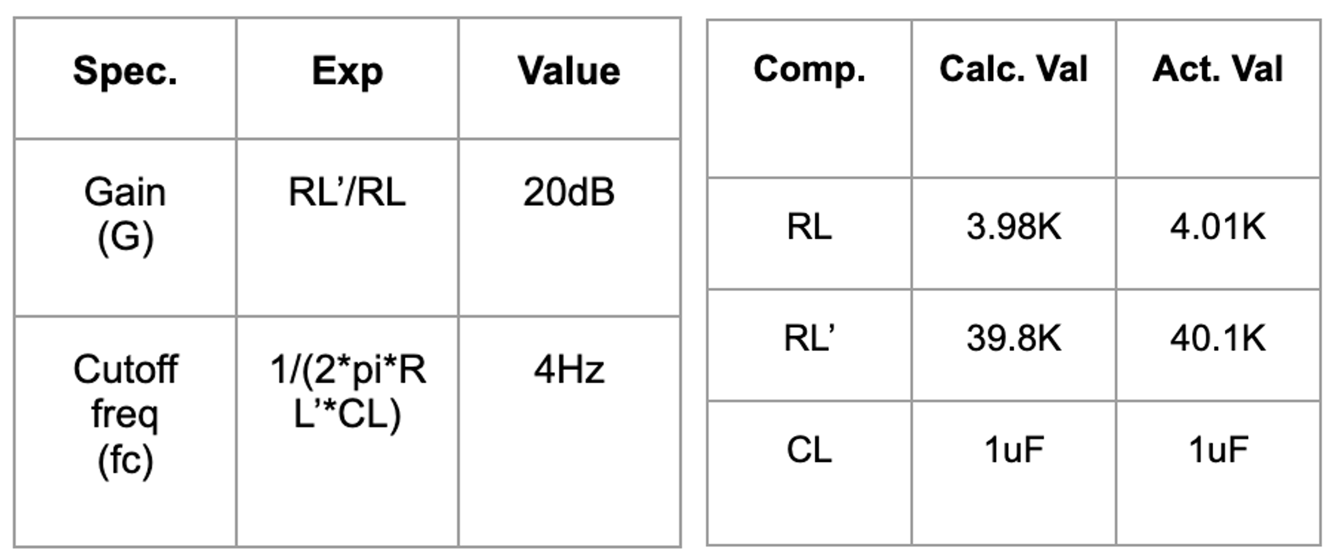
Fig.3 - Filter Calculations (BPF)
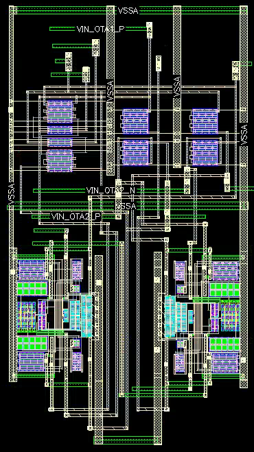
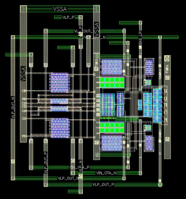
Fig.4 - BPF Layout
The figure above depicts the layout of the BPF used for the HR stage. Going by area requirements and ease of implementation, only HR passives were fabricated on-chip, and subsequently the filtering stage for HR. This layout incorporates the FDA layout as is and builds a BPF using passives.
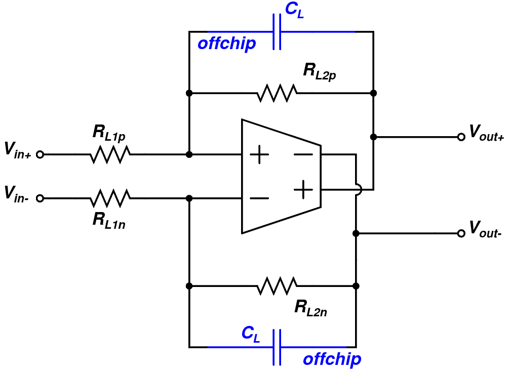
Fig.5 - LPF Schematic
Similar to the BPF for both paths, the LPFs for both paths have an off-chip capacitance of 1uF. Appropriate values of resistors were used to obtain a 3dB BW of 4 Hz and 0.4 Hz for HR and BR paths, respectively. The values of passives and the gain obtained for each path through this LPF is outlined in the tables included below.
Fig.6 - LPF Testbench
Fig.7 - HR LPF Calculations
Fig.8 - LPF Layout
The figure above depicts the layout of the LPF used for the HR stage. Going by area requirements and ease of implementation, only HR passives were fabricated on-chip, and subsequently the filtering stage for HR. This layout incorporates the FDA layout as is and builds a LPF using passives.
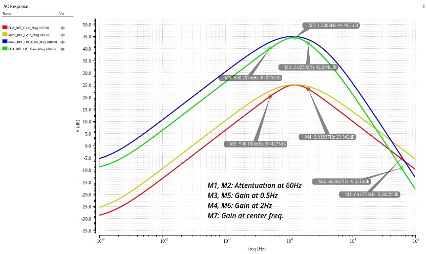
Fig.9 - BPF & LPF AC Response
The figure above compares the HR BPF & LPF AC response obtained using ideal blocks and blocks designed using active components (i.e., transistor based FDA's). While gain at the center frequency is similar for both cases, the simulated 3dB BW for the active blocks are lower in comparison to the ideal blocks. This can be attributed to additional parasitics that stem from the transistor-level FDA's. This particular reduction in bandwidth is acceptable as the 3dB BW is still wider than the actual signal bandwidth for HR.