
Transmitter Design
The purpose of the TX system is to take 2.56MHz and 40KHz as input clocks, along with the trigger signal from the FPGA and various control signals from the SPI block as inputs, to generate 4 outputs. Each output is a periodic sequence of pulses at 40KHz used to drive the off-chip power amplifier on the PCB. The phase and the number of pulses at each output can be digitally programmed from the SPI block. The TX system requires a trigger signal from the FPGA to know when to produce the pulse sequences.
The TX system consists of four blocks: i) a Sequence Generator, ii) a Phase Generator, iii) an Envelope Extender, and iv) an Output Buffer. This section explains the details, functionalities of each block, and how they are connected.
Sequence Generator
The Sequence Generator is a circuit block that generates a specific number of pulses at 40KHz based on the instruction from the SPI block. This is primarily obtained by 3 main sub-blocks: i) a 2-1 MUX, ii) a 5-bit Counter, and iii) a Digital Comparator. The connections of these blocks are illustrated in the following schematic.
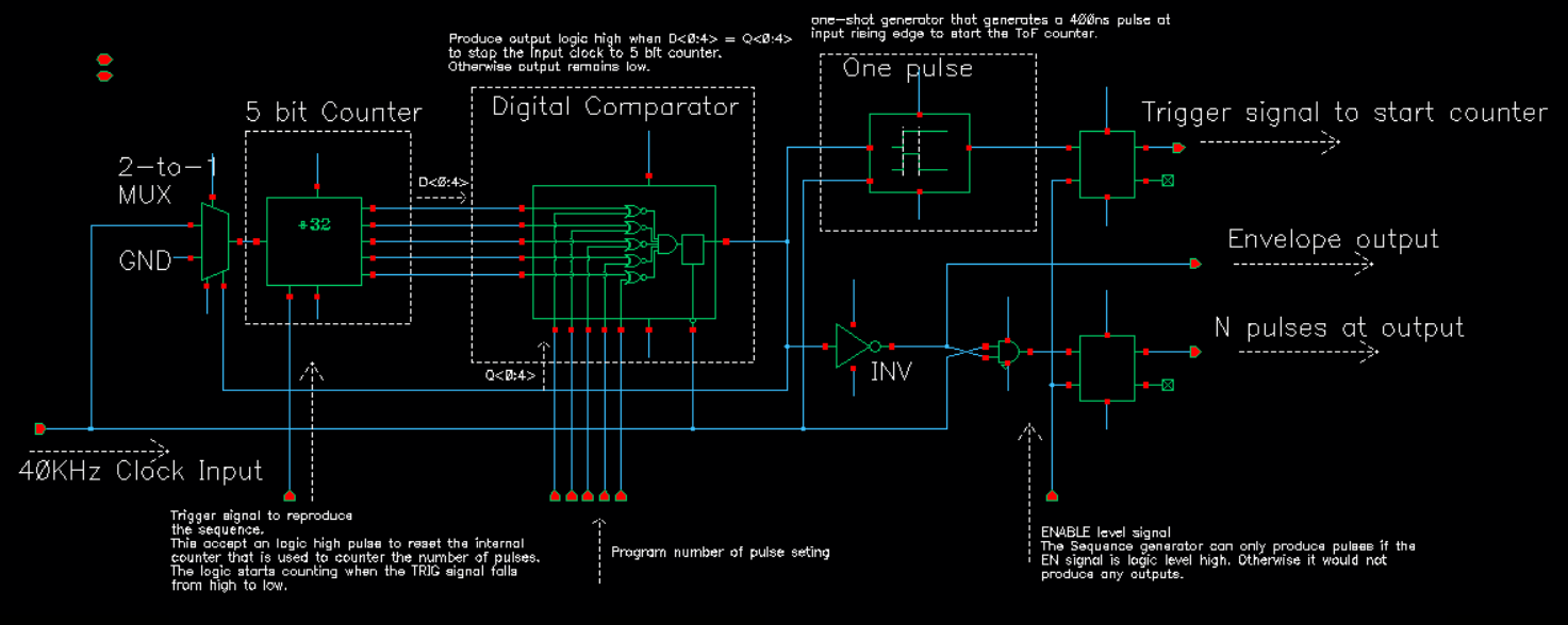
Figure 1. Sequence Generator schematic.
The Digital Comparator is the most crucial logic block so it will be explained first. The purpose of the Digital Comparator is to compare if the two 5-bit binary numbers at its inputs are matched. It will produce a logic 1 if the two numbers are equal, and a logic 0 if the two numbers are unmatched. The Comparator takes the first number as the target number of pulses, which is programmed by the SPI, and the second number as the number of pulses being counted in the current sequence. The Digital Comparator is implemented by using 5 NXOR logics to compare 5 pairs of corresponding bits in the two numbers. If any NXOR logic sees a difference in its two inputs, it will produce a logic 0 at the output, which subsequently makes the Comparator produce a logic 0. On the other hand, if none of the NXOR sees a difference in its two inputs, they all will produce a logic 1, and the Comparator will produce a logic 1 at the output.
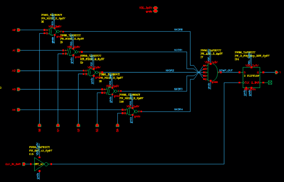
Figure 2. Digital Comparator schematic.
The second most important block is the 5-bit Counter, which is used to count the number of pulses in the current sequence. This is a synchronous design similar to the Clock Divider circuit mentioned previously.
The pulse generation process is initialized when the FPGA sends a trigger signal to the chip. The 5-bit Counter receives the trigger signal and sets all output bits to 0s. These Counter outputs are connected to the inputs of the Digital Comparator. The Digital Comparator detects the difference between the Counter outputs and the SPI outputs, which are used to set the desired number of pulses, and produces a logic 0. This logic is sent to a 2-to-1 MUX, which subsequently selects the 40KHz clock input and feeds it to the 5-bit Counter. The cycle repeats as the Counter counts the number of pulses incrementally.
The cycle stops when the Counter outputs reach the desired number of pulses programmed by the SPI. When this happens, the Digital Comparator flips its output from 0 to 1. This logic 1 is sent to the MUX, which in turn feeds logic 0 to the Counter and stops the counting process. Both the Counter and the Digital Comparator will be in the freeze state until the next trigger signal from the FPGA is sent to the Counter, which resets all of its output to 0s to feed the 40KHz clock to the Counter again.
Throughout this pulse generation process, notice that the invert of the output of the Digital Comparator acts as an envelope of the pulse sequence. It is 1 when the sequence is generated, and 0 when the sequence is not generated. Therefore, the Digital Comparator output is inverted and AND with a 40KHz clock to generate the 40KHz pulse sequence.
To avoid any problem related to race conditions and setup/hold time, the Digital Comparator changes its output state at the falling edge of the 40KHz clock, while all other circuits in the Sequence Generator are synchronized to the rising edge of the clock.
Phase Generator
The Phase Generator takes the pulse sequence from the Sequence Generator as input and generates 4 pulse sequences at its outputs, each output can be programmed to have a specific phase by the SPI. The phase delay has a resolution of 5.625 degrees and the range is from 0 to 331.875 degrees. The Phase Generator comprises two main sub-blocks: i) a Tapped-Delay Line and ii) 64-to-1 MUX as described in the following diagram:
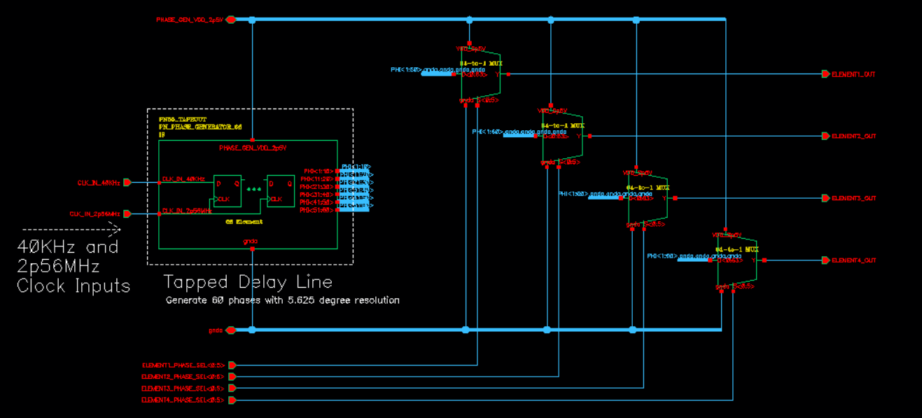
Figure 3. Phase Generator schematic.
The Tapped-Delay Line consists of 60 D flip-flops connected in a cascade manner: the input of the first flip-flop is connected to the output of the Sequence Generator block, and the output is connected to the input of the second flip-flop, and so on. All flip-flops share the same 2.56MHz clock. By doing so, the outputs of the two consecutive flip-flops are delayed by 5.625 degrees, and 60 D flip-flops can cover a range of 331.875 degrees.
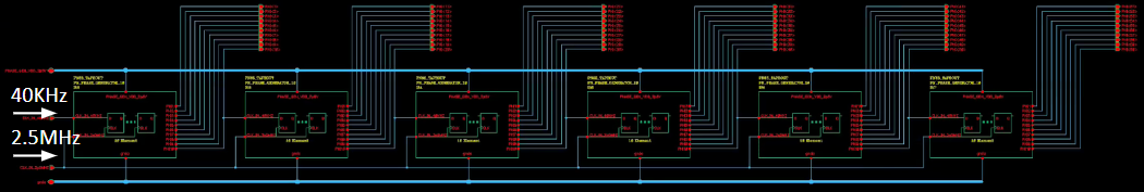
Figure 4. Tapped-Delay Line schematic.
The output of each D flip-flop is routed to a corresponding input of the 64-to-1 MUX. The MUX selects which inputs to be routed to the output, and therefore, decides the phase at the output. There are 4 MUXes in total corresponding to 4 outputs.
Envelope Extender
The Envelope Extender is added to the TX block as a way to turn off the RX LNA when the TX transmits high-power signals. Turning off the LNA is crucial as we do not want the signals from the TX side to couple to the RX inputs and saturate the RX, producing false detection. When the TX generates waveforms at the output, the Envelope Extender block sends a logic signal to turn the LNA at RX to turn off the LNA gain. The LNA remains off a programmable amount of time after the TX finishes generating the waveforms at output, which ensures that all of the high-power signals are launched far away from the board. Only at this time, the Envelope Extender flips the logic and turns on the LNA gain. The logic of the Envelope Extender is similar to the logic of the Sequence Generator and the schematic diagram is described below.
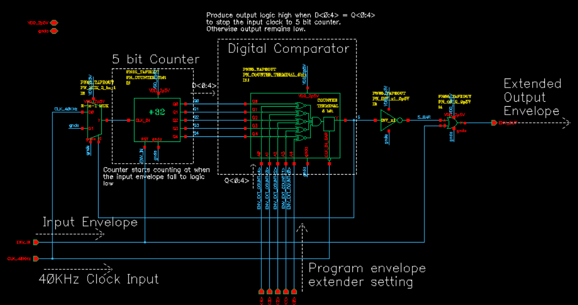
Figure 5. Envelope Extender schematic.
Output Buffer
The on-chip output buffer blocks are used to drive the off-chip power amplifiers, each of which has a large input capacitance of around 640pF (SH8MA4). Each buffer consists of x4, x8, x16, x64 inverters connected in cascade. The sizes of the x64 inverter are 64um for NMOS and 128um for PMOS.
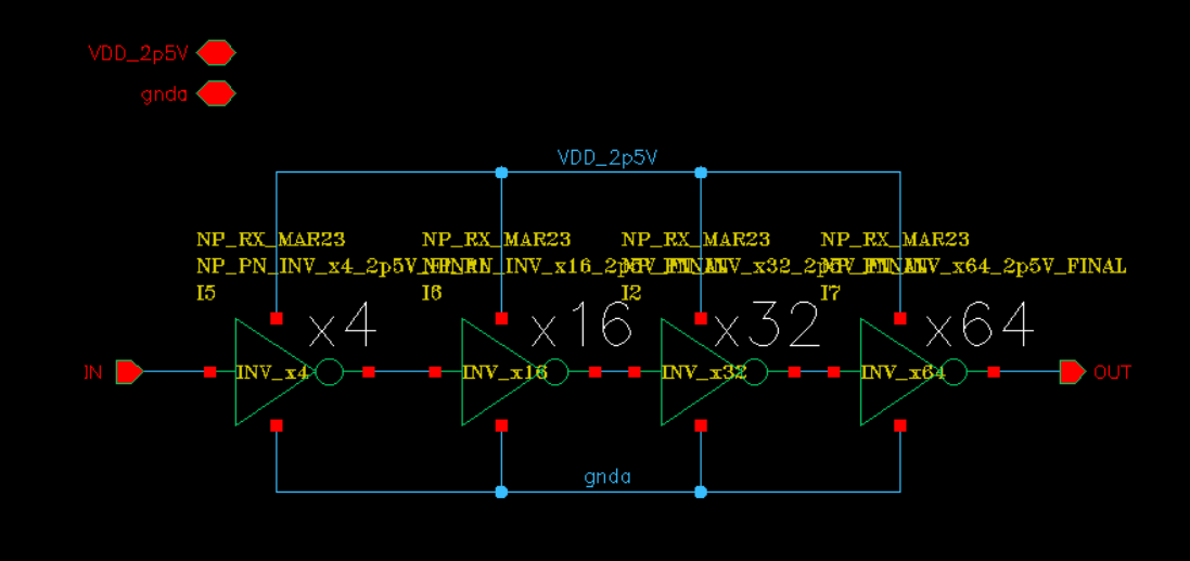
Figure 6. Output Buffer schematic.
Transmitter System
The whole diagram of the TX architecture is shown below. It starts with the Sequence Generator to generate the pulse sequence, followed by a Phased Generator to achieve a proper phase at the output. Finally, the output buffer is used to drive the large load off-chip power amplifiers. There is also an Envelope Extender circuit to turn off the LNA at the RX when the TX produces waveforms at output. Any input connected to an external bonding wire has a Schmitt trigger acting as a buffer to filter out the ringing effect from the bonding wire.
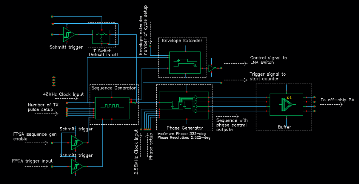
Figure 7. Transmitter system.
Clock System
The whole chip needs two clock frequencies to operate: a 2.56MHz clock used in the TX?s Phase Generator block and a 40KHz clock shared between TX and RX?s Counter blocks. To generate these two clocks, the chip takes a 5.12MHz clock externally from the FPGA and passes through a Schmitt trigger circuitry to eliminate the ringing effect from bonding wires, before passing to a clock divider block. The clock divider consists of 7 JK flip-flops connected in a synchronous manner; each flip-flop subsequently takes the clock at its J input and produces another clock at its K output with the frequency divided by half. The outputs of the 1st and 7th flip-flops are taken out as the 2.56MHz and 40KHz clocks. These clock signals are routed on the top wide metal layer to the desired location across the chip to minimize RC delay.
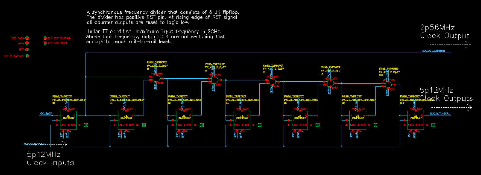
Figure 8. Frequency divider schematic.
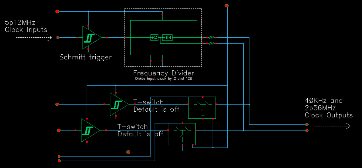
Figure 9. Clock system.
Transmitter System Simulation
The figure 10 below shows 40KHz square waves at the D-output of the 1st, 10th, 20th, 30th, 40th, and 60th D-flip-flops in the Tapped-Delay Line. We can see that the square waves retain their shape and the only difference between traces is the delay between them. The maximum delay that can be achieved with this Tapped-Delay Line approach is ~332 degrees, and the minimum phase delay or phase resolution is 5.625 degrees.
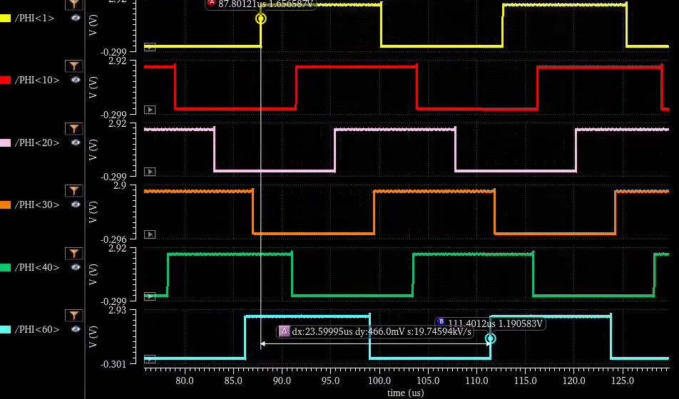
Figure 10. Tapped-Delay Line simulation.
The figure 11 below shows all the important signals that the TX system takes as inputs and outputs. The blue line on the top row is the trigger signal from the FPGA to trigger the TX to generate waveforms. Right after the TX receives the trigger signals, it generates four 40KHz waveforms at the output as shown in the red, pink, orange, and green traces. In this example, all the outputs are set to have a 0-degree phase.
After the TX completes generating waveforms, it produces a trigger signal, the yellow trace in the figure, to send to the counter to start the counting process, which is used to estimate the distance to the detected object. During the TX transmitting process, the LNA at the RX system is off because the gain control signal, the purple trace, is off. After a long enough amount of time, the TX flips the logic of the purple trace to make it on and turn on the LNA.
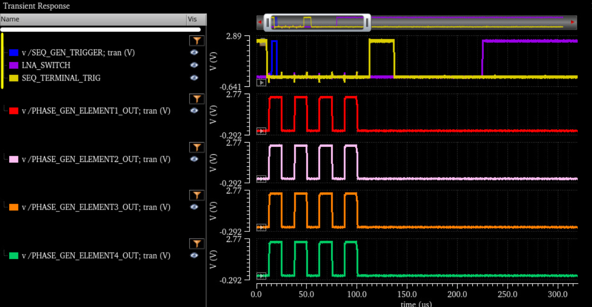
Figure 11. TX system simulation.