
PCB Design and Layout
PCB Design
The PCB is designed using a two-layer board with FR4 substrate. The PCB is divided into the following regions:
-
Power and connector
-
Biasing circuit
-
Level-shifter
-
Chip socket and RX transducer
-
Power amplifier and TX transducers
The power and connector region consists of multiple LDOs producing supply voltages at 3.3V, 2.5V, and 1V. The input of these LDOs is connected to a barrel connector that accepts an input voltage of 4.5V. Each LDO comes along with a switch to turn off and on any specific power domains in the chip for testing purposes.
The biasing circuit consists of various potentiometers that are used to set the current bias of the chip. The package of these potentiometers is chosen such that it has robust knobs to reduce the chance of accidentally being adjusted when hands touch the board. For each potentiometer, there are parallel SMD pads in place so that a fixed resistor can be soldered in place of a potentiometer once the value of the potentiometer is determined.
The level-shifter circuits are used to translate from an FPGA’s 3.3V logic to chip 2.5V logic. The level-shifter IC is chosen such that it can work bi-directionally, meaning that the logic signal can travel both from the FPGA to chip and from chip to FPGA. There are jumpers at the outputs of the level-shifter to enhance the reconfigurability in case any level-shifter chip fails and needs to be isolated from the rest of the PCB.
The region contains the chip socket and the RX transducer is placed at the center of the chip. The socket solution is used in this PCB to obtain two benefits. The first benefit is to reduce footprint area compared to surfboard configuration and the socket footprint is not significantly larger than QFN surface mount. The second benefit is to enhance the reconfigurability compared to a straight solder solution: In case the chip is burnt or defunct, a new chip can be conveniently replaced and the testing procedure can start right away. Surrounding the chips are bypass capacitors to reduce the level of ripple in biasing and supply nodes.
The power amplifiers section is placed on the bottom right side of the PCB, and the TX transducers are placed on the right edge of the PCB. TX and RX sensors are placed far apart to ensure an appropriate distance between them, which practically reduces the direct coupling power level when the TX is on.
On top of that, there are a few details that are worth mentioning. There is a row of ground vias that surround the chips. This row acts as a ground wall to prevent the RF signal from leaking through the side of the board. Ground headers and jumpers are added at strategic locations on the PCB to enhance the reconfigurability of the board and ease of debugging.
PCB schematic designs.
Off-chip Power Amplifier
To boost the power of the output signal for far-range scanning, the TX signals are amplified with off-chip power amplifiers. The purpose of these amplifiers is to take 2.5V peak-to-peak signals as inputs and amplify them to 15V peak-to-peak signals at output. These output signals are then used to drive the off-chip transducer (MA40S4S), which can handle 20V peak-to-peak swing.
The off-chip power amplifier is a two-stage amplifier. The first stage consists of an NMOS switch in a shunt configuration with a pull-up resistor. The purpose of the first stage is to convert a 2.5V peak-to-peak signal to a 15V peak-to-peak at output. Converting a low-level digital signal to a large signal requires a device that has a low threshold voltage while sustaining a large voltage swing at the output or high Drain-Source break-down voltage. The Rohm Semiconductor?s SH8MA4 is chosen as it has a threshold voltage of 2.5V maximum and a Drain-Source breakdown of 30V.
The second stage is a push-pull amplifier with a PMOS on the high side and an NMOS on the low side. The push-pull driver is used to enhance the driving capability of the output driver, which needs to drive a large capacitance of 2.2nF. To limit the shoot-through current that can burn the devices during the transition period, or when both NMOS and PMOS are on at the same time, 100-ohm resistors are connected in series at the output.
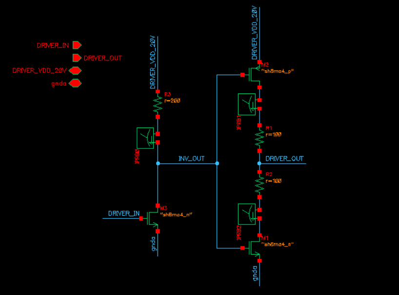
Figure 1. Power amplifier schematic.
PCB Layout
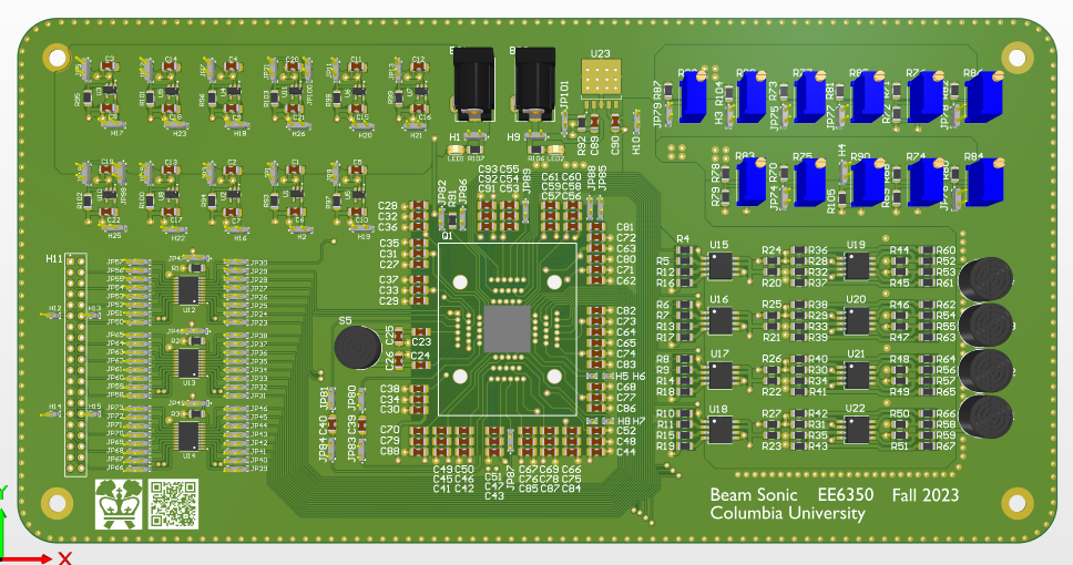
Figure 2. Front view of PCB.
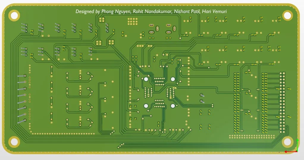
Figure 3. Back view of PCB.
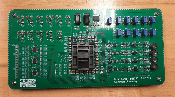
Figure 4. PCB when fully populated.