
Hierarchical Design and Chip Floorplan
Power Domain
For ease of debugging and reconfigurability, the whole chip is divided into 10 power domains by power cut lines. During the testing process, only one block under-test is turned on at a time. If there is any failure existing within a block that prevents the proper functionality of the block, we have the flexibility to turn off that block and avoid contaminating other blocks. The following list shows the power domains with corresponding VDD levels:
-
Envelope Extender (2.5V power level)
-
Sequence Generator (2.5V power level)
-
LNA + PGA (2.5V power level)
-
Mixer + Comparator (2.5V power level)
-
Counter (2.5V power level)
-
IO (2.5V power level)
-
Frequency Divider (2.5V power level)
-
Switch + Buffer (2.5V power level)
-
Phase Generator (2.5V power level)
-
SPI (1V power level)
Hierarchical Design
The design is placed in a hierarchical order for ease of management. Each cell within the design hierarchy can have multiple schematic views so that the debugging and testing process is easier and quicker. For example, the TX system cell has two views: one with SPI and another without SPI. Both of these views are saved in the same cell and the view configuration is managed by Config View in Cadence. The multiple views are utilized so that the rest of the TX system and the SPI functionalities can be tested separately. The hierarchy has 6 levels with level 6 being the highest and level 1 being the lowest. The design views from Level 3 to Level 6 are illustrated below.

Figure 1. Level 6 - Top chip with bonding wires.
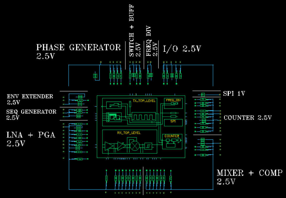
Figure 2. Level 5 - Top chip with ESD pads and power cuts.
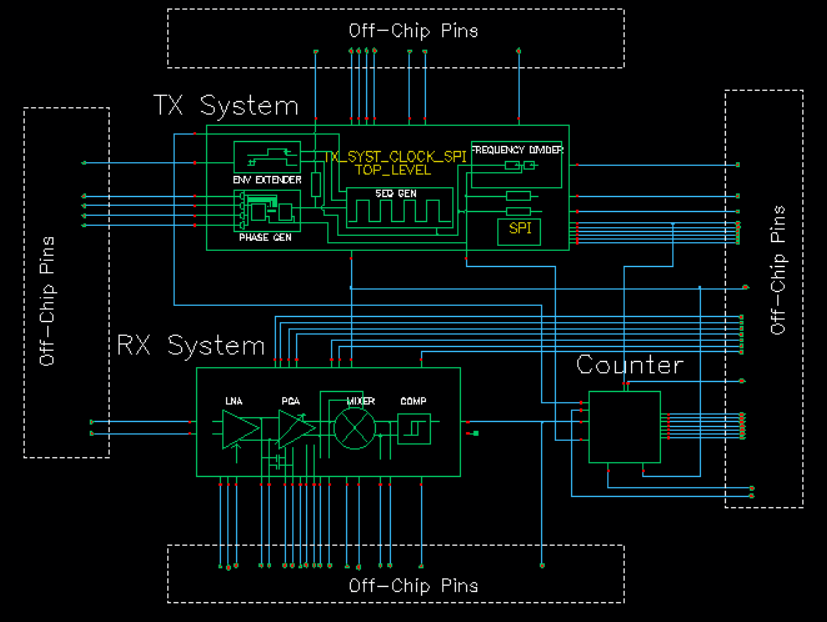
Figure 3. Level 4 - Top chip design.
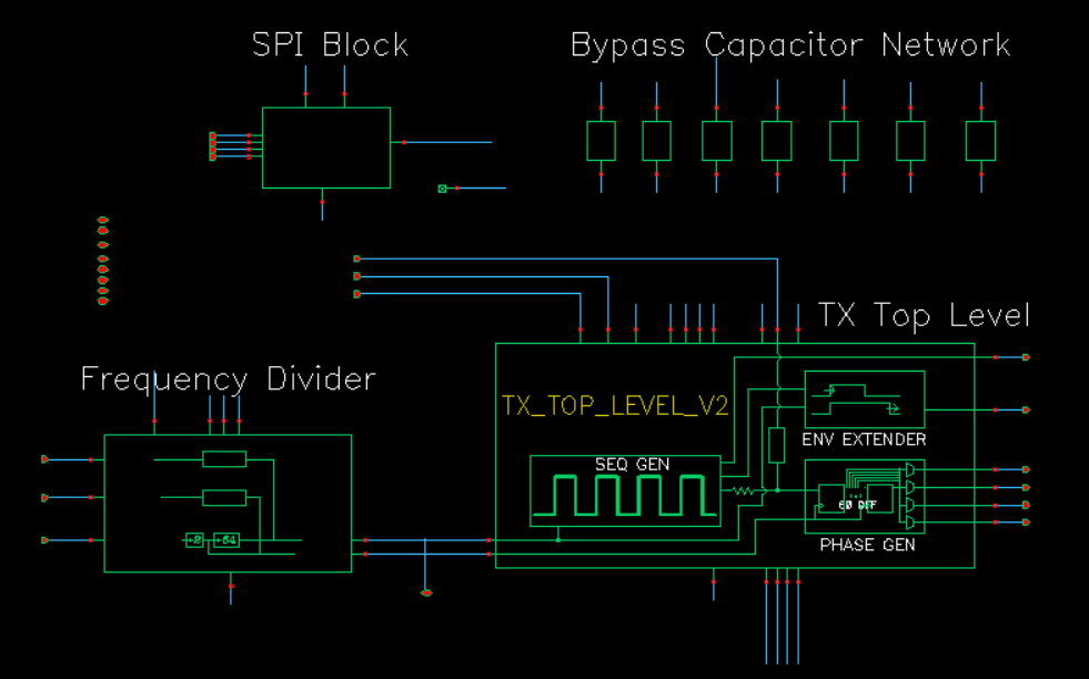
Figure 4. Level 3 - TX system with SPI and Clock Divider system.
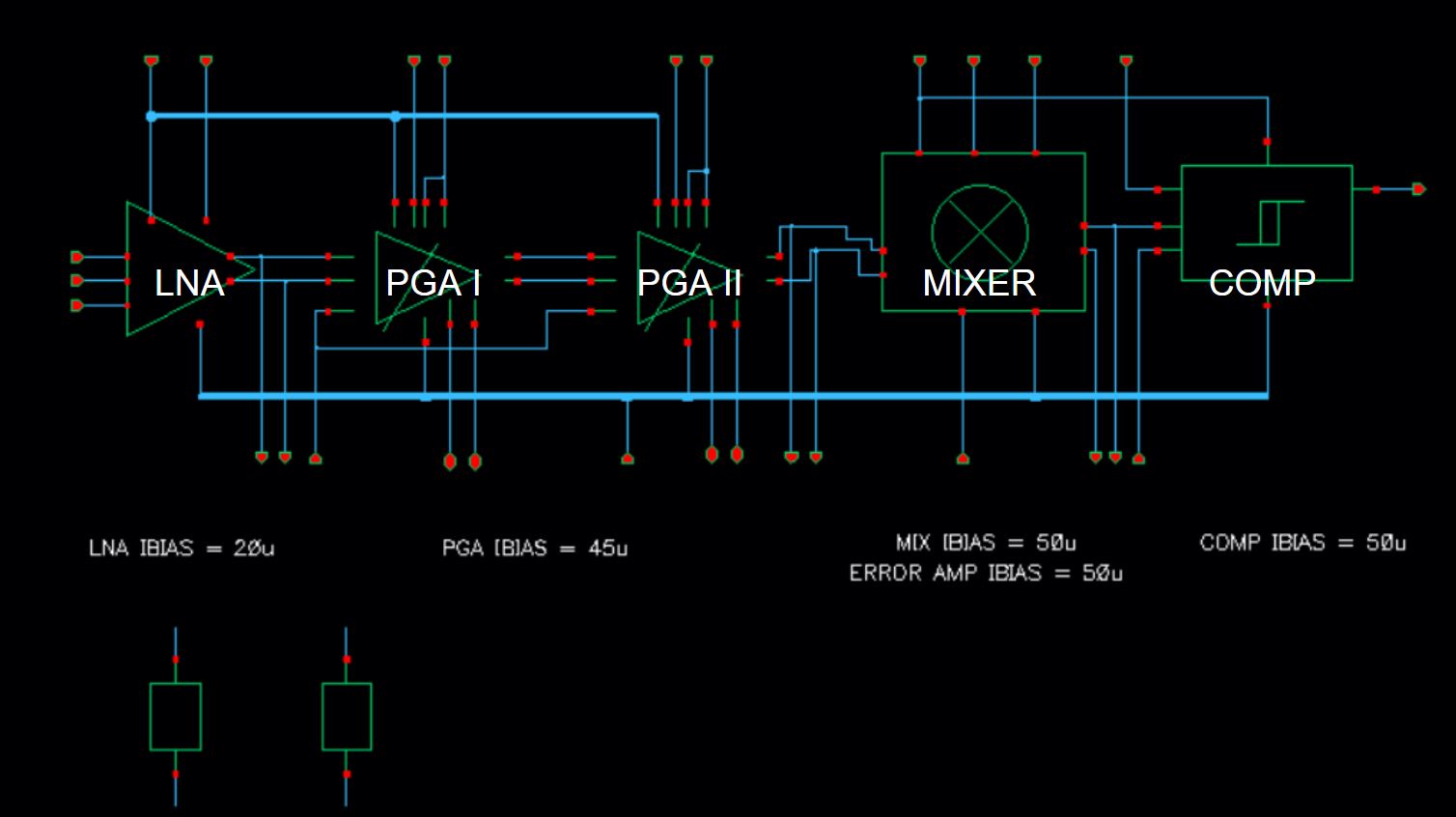
Figure 5. Level 3 - RX system.
Chip Floorplan
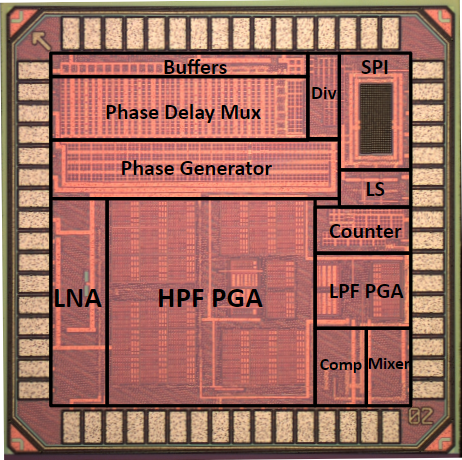
Figure 6. Chip floor plan.
The whole chip has an area of 1mm x 1mm. The TX and RX systems are clearly divided with TX on the North side and RX on the South side. This isolation is employed to ensure that the digital-intensive actions from the TX do not couple to noise-senstive RX.