System Simulations and Measurements
System Simulations
System Simulation Testbench
Before the tapeout submission, the design of the chip has to pass the functionality test. The following section illustrates the details of the system testbench, where the chip is placed in an environment close to the interface between the chip and PCB and sensors. The testbench consists of several modules:
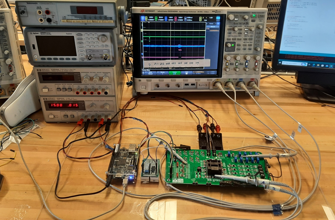
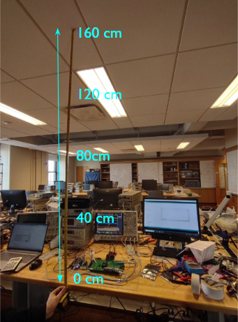
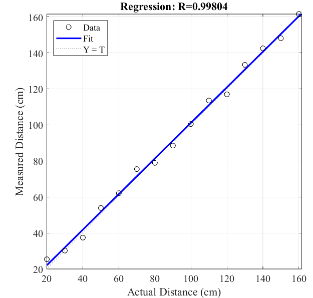
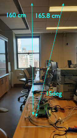
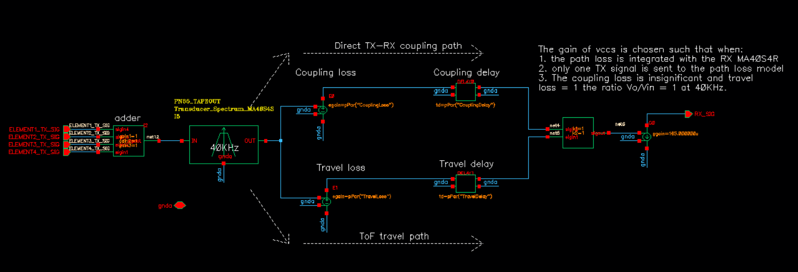
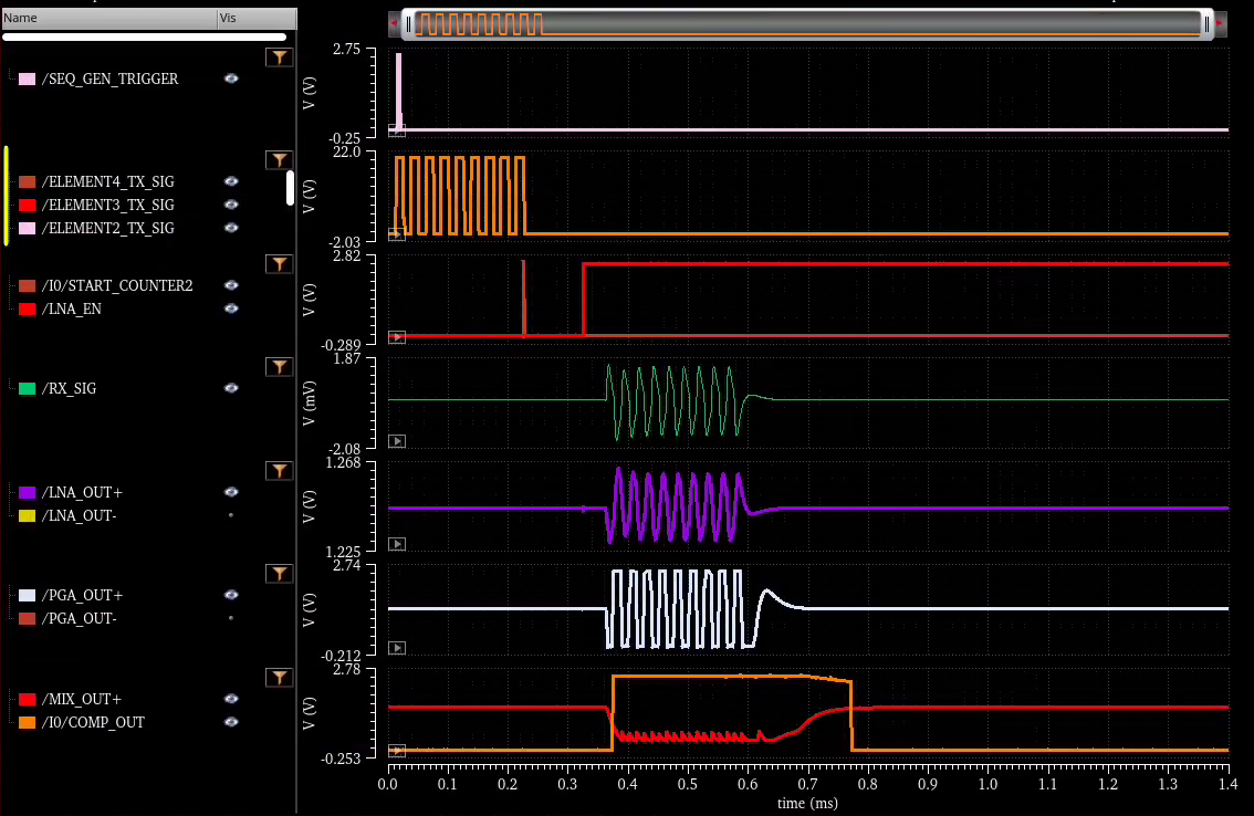
Figure 1. System simulation testbench. BeamSonic IC: This is the module that contains the complete design of the IC. This module includes ESD pads, bonding wire inductive effects, and other packaging effects. VDD Supply: this module contains multiple voltage supplies to provide 2.5V and 1V to power the IC. RX Biasing: This module contains various current and voltage sources to provide the proper biasing to LNA, GPA, and other circuitries in the RX system. It also has a SAR ADC, which is used to convert from decimal value to binary, to program the gain of the PGA. FPGA: This module includes signal sources to transmit the trigger signals to the IC. It also includes a 5.12MHz clock signal that is used as the reference clock of the chip. Off-chip Power Amplifier: This module includes 4 off-chip power amplifiers. Path-loss model: This module emulates multiple physical transmission effects from TX to RX, including the beam-forming, direct-coupling, and attenuation effects. The design of the model is described in the figure below. It takes 4 TX signals generated by TX transducers as inputs and adds them together using an adder circuitry. It then passes the summed signal to a 40KHz 2nd-order bandpass filter. This filter is used to emulate the frequency response of the MA40S4S transducer and can be found in the datasheet. Then the signal is split into two different paths; each path consists of an attenuator element and a delay element. The first path is called the direct TX-RX coupling path, where it represents the direct coupling path between TX and RX. In this path, the attenuation level is set to 10dB and the delay is set to 10us. The second path is called the Time-Of-Flight path, where it represents the signal path that travels from TX to the detected object and bounces back to the RX, therefore, the attenuation level is set to larger at 40dB and the delay is longer at 350us. Figure 2. Environment path loss model. System Simulation Results The figure below shows a list of important signals the Beam Sonic chip generates. On the 1st row we see the trigger signal sent from the FPGA, and right after that on the second row are the 4 output signals from the off-chip power amplifier; each has 8 pulses at 40KHz with an output swing of 20V peak-to-peak. The brown line on the third row is the trigger signal to start the counter, which comes right after the TX output completes the pulse generation, and after a certain period is the LNA_EN signal, which is used to turn on the RX?s LNA. Row 4th, 5th, and 6th are the signals at the RX input, LNA outputs, and PGA outputs. Finally, the 7th row contains the outputs of the mixer and comparator. The system simulation shows every waveform behaves as expected. Figure 3. System simulation results. Measurement Setup The whole system consists of a controller FPGA, PCB, and a perf board to control the PGA gain. All of them are glued on an acrylic board to enhance system robustness. Four oscilloscope probes are used to measure signals at various locations: including the FPGA trigger signal, off-chip power amplifier output, PGA output, and comparator output. The system and zoom-in waveforms view are shown in the figures below. The probes and cables are also glued to the acrylic board to reduce unnecessary cable movement that can loosen the contact between the probes and PCB connections. Figure 4. The system is glued on an acrylic surface. Figure 5. Zoom-in view of important waveforms on PCB. Range Measurement Figure 6. System measurement setup with a ruler. The whole system is placed on a flat table in the teaching lab and faces upward. A plastic lid is placed above the system at different heights to act as an object of interest, and a ruler is used to measure the distance between the lid and the PCB. We record the actual distance, which is measured using a ruler, and the measured distance, which is recorded from the radar system based on the delay between the trigger signal and the comparator. The measurement results are recorded in the plot below: Figure 7. Actual distance and measured distance. The measured distance follows a linear line, with a regression coefficient of 0.99804. This indicates that the system can measure both close-range distance and far-range distance with consistent accuracy. Beamforming Measurement Figure 8. Setup to measure beamforming effect. We also attempt to measure the beamforming effect by still pointing the beam upward and using the ceiling in the teaching lab as an object of interest. We program the beam to change from 0 degrees to 15 degrees and expect to see the range change from 160 cm to 165.8 cm. However, the difference between the two measurements is barely noticeable in the oscilloscope. In the future, this difference can be demonstrated if the system can be brought outdoors, where the distance between objects and the system is much larger than 160cm.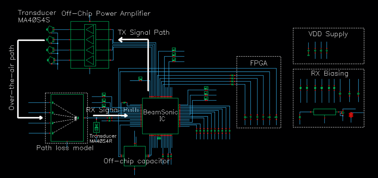
System Measurements