
Receiver Design
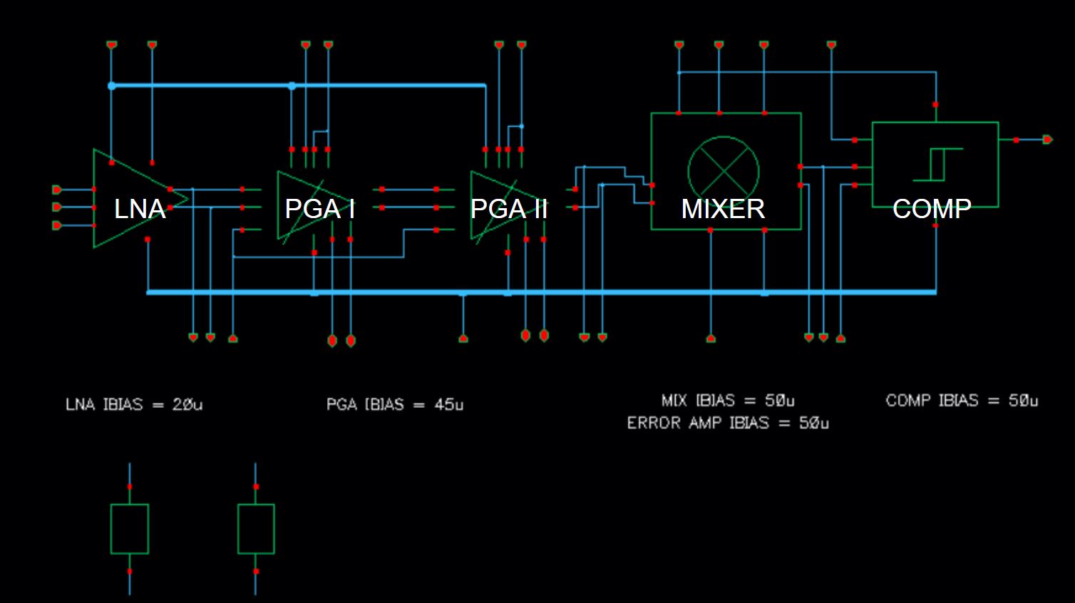
Figure 1. Receiver system.
Low Noise Amplifier
Sensitivity of the whole receiver is largely determined by the low noise amplifier (LNA). An ideal LNA will add gain to the signal while adding minimum noise. Noise contribution of LNAs in standard 50 ohms RF systems is defined in terms of Noise Figure (NF). However, in our project, since the sensor is not 50 ohms impedance, we reported input referred noise power density. The designed LNA has a voltage gain of 27.73 dB with input referred noise voltage of 4.24 nV/sqrt(Hz).
The implemented LNA is a simple differential amplifier with resistive load. We tried active load but it was adding more noise without increasing gain by a significant amount. High VDD was helpful to load LNA with a higher resistor, which gave required higher gain. Ultrasonic sensor is attached differentially to the LNA. On-PCB DC block capacitors are used and LNA input is biased using the current mirror. The bias current of LNA can be changed to tackle process variations.
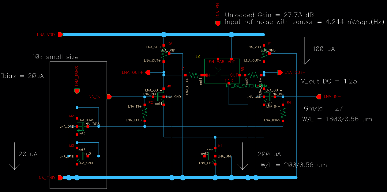
Figure 2. LNA schematic.
Since we are operating at lower frequencies, flicker noise was the major issue while designing the LNA. We solved this problem by using large device sizes which pushed flicker noise corner to lower frequency (< 1 KHz). Secondly, we optimized LNA design for lower power consumption. High Gm/Id = 27 is achieved while maintaining noise, gain and linearity tradeoffs. LNA consumes 220 uA (200uA + 20uA bias) current at 2.5 V supply.
Programmable Gain Amplifier
This forms the part where the range of the Radar is controlled by adjusting the gain of the Front-End. The gain control can switch gains from 0 dB to 80 dB. The spot noise at Programmable Gain Amplifier (PGA) input is about 11.8 nV/√Hz. There are two stages in the PGA.
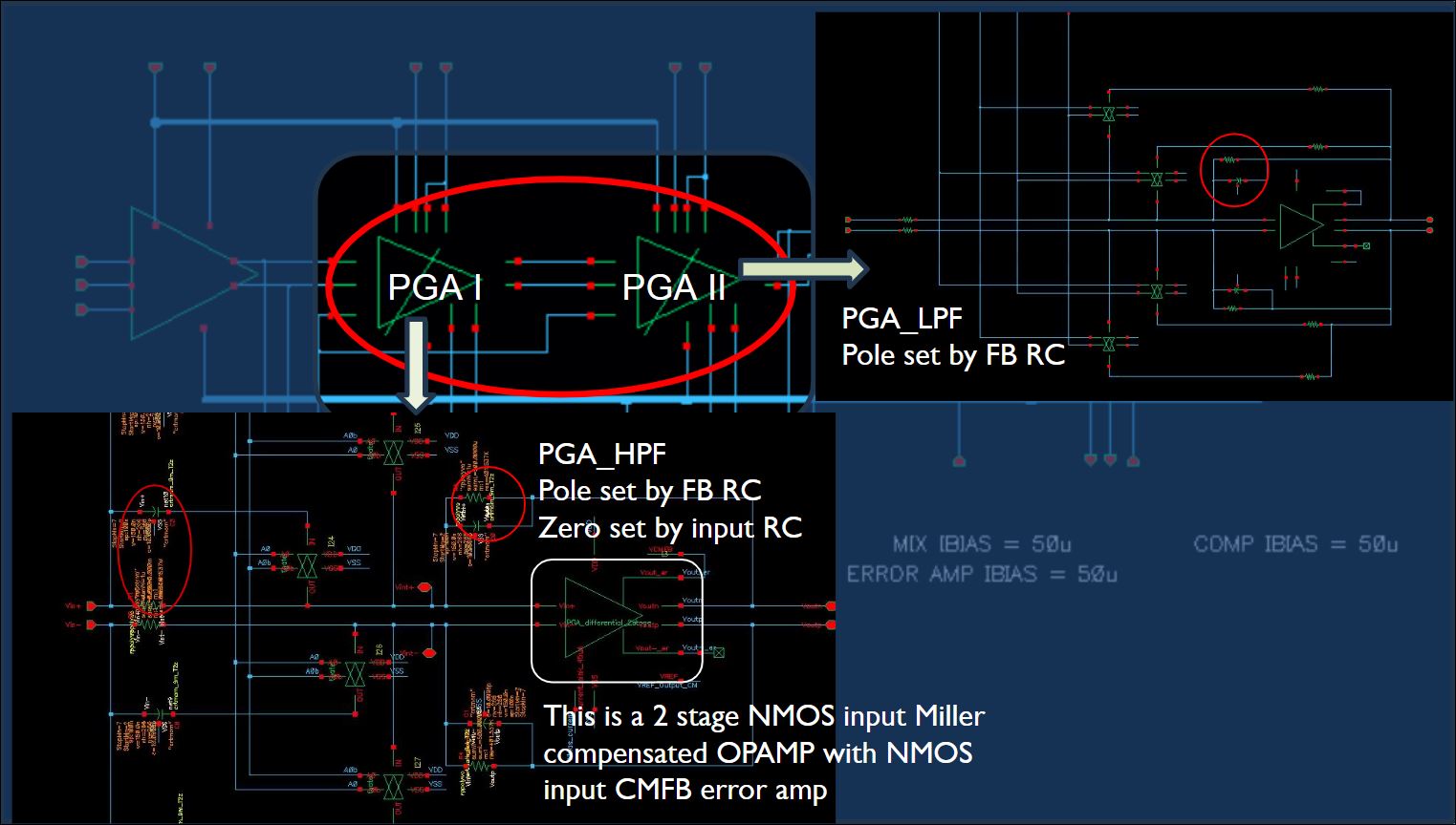
Figure 3. PGA schematic.
The first stage forms a high pass filter designed to reduce the integrated noise rms at the input and avoid flicker noise from PGA. The first stage gain is set by the capacitors in the feedback arm and the inverting arm of the amplifier. The maximum gain (Typ) for this stage is 40 dB.
The second stage forms the Low pass filter to reduce the high freq part of integrated noise thus creating a net band pass response centered at 40 kHz. The gain is set by the ratio of the resistors in the feedback arm to inverting arm of the amplifier. The maximum gain (Typ) for this stage is 40 dB.
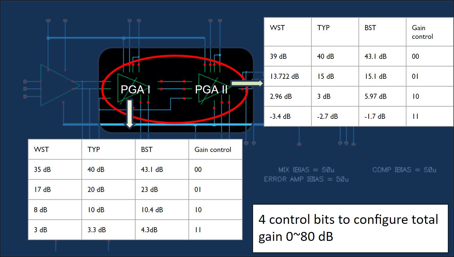
Figure 4. PGA gain control setting.
Now, to understand the design the amplifier, let us take a look at the below image. It is a common-mode feedback (CMFB) based Differential two-stage Miller Compensated OTA. The bias current is set externally (using a resistor off-chip)for additional control. The error amplifier is a differential input amplifier with diode load. We set the output CM externally for the mixer stage. Note that the widths are large to further reduce input referred flicker noise. As already stated, we achieve a input referred spot noise of 11.875 nV/sqrt(Hz)at 40 kHz which is crucial to achieve the specifications calculated.
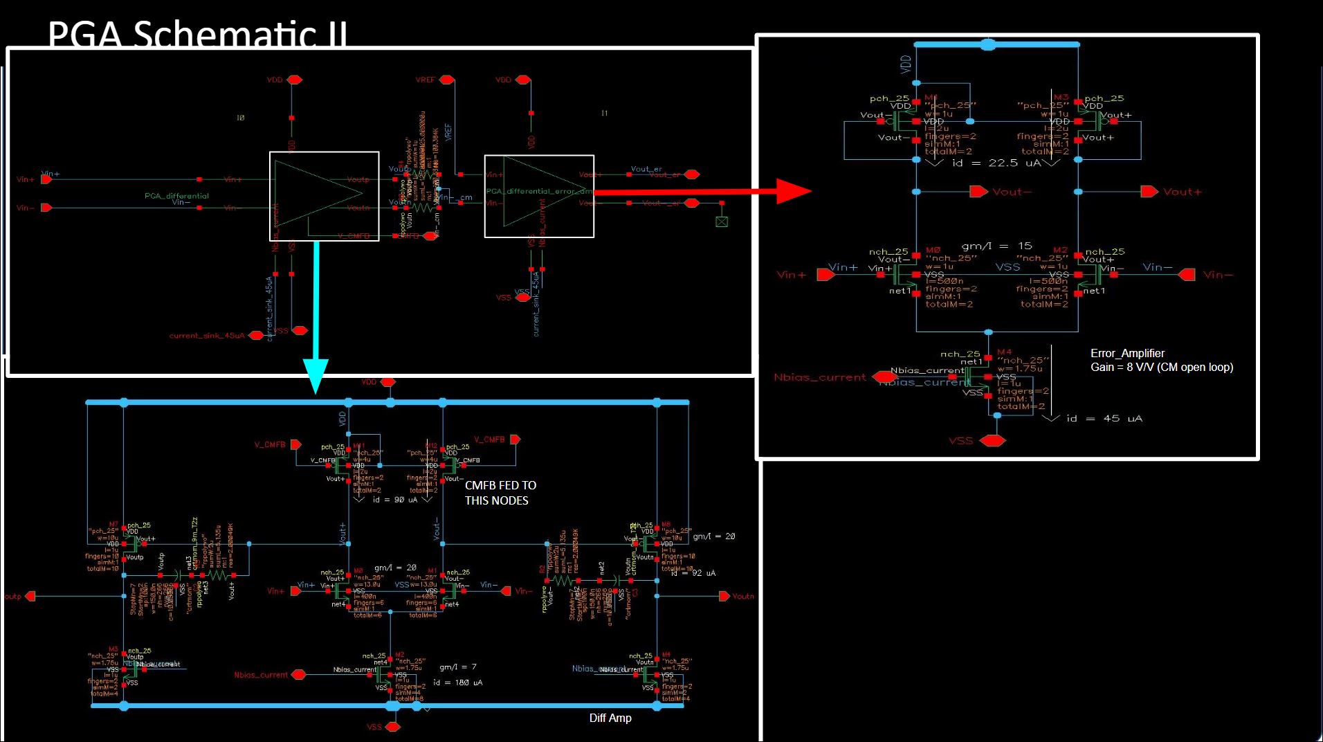
Figure 5. PGA CMFB schematic.
Self Mixing using Gilbert Cell Mixer
The PGA output will have a 40 KHz signal when the receiver sensor detects an object, else will be simply DC biased constant voltage. We can treat it as an amplitude modulated signal at 40 KHz. A simple way to demodulate this signal is by means of self mixing. In self mixing, we are mixing PGA output with itself. When the PGA output is constant, ie, no object is present, we get a constant bias voltage at the mixer output. When PGA output is a 40 KHz signal, mixing of 40 KHz with itself will give us DC and a signal at 80 KHz. In the time domain, it looks like a pulse of 80 KHz signal with an amplitude envelope. The amplitude of the envelope is directly proportional to PGA output 80 KHz amplitude. If we simply add a large capacitor at the mixer output, which creates a low pass filter response to filter out 80 KHz signals, we get a DC envelope. Which can be used by the comparator to make a decision on object detection.
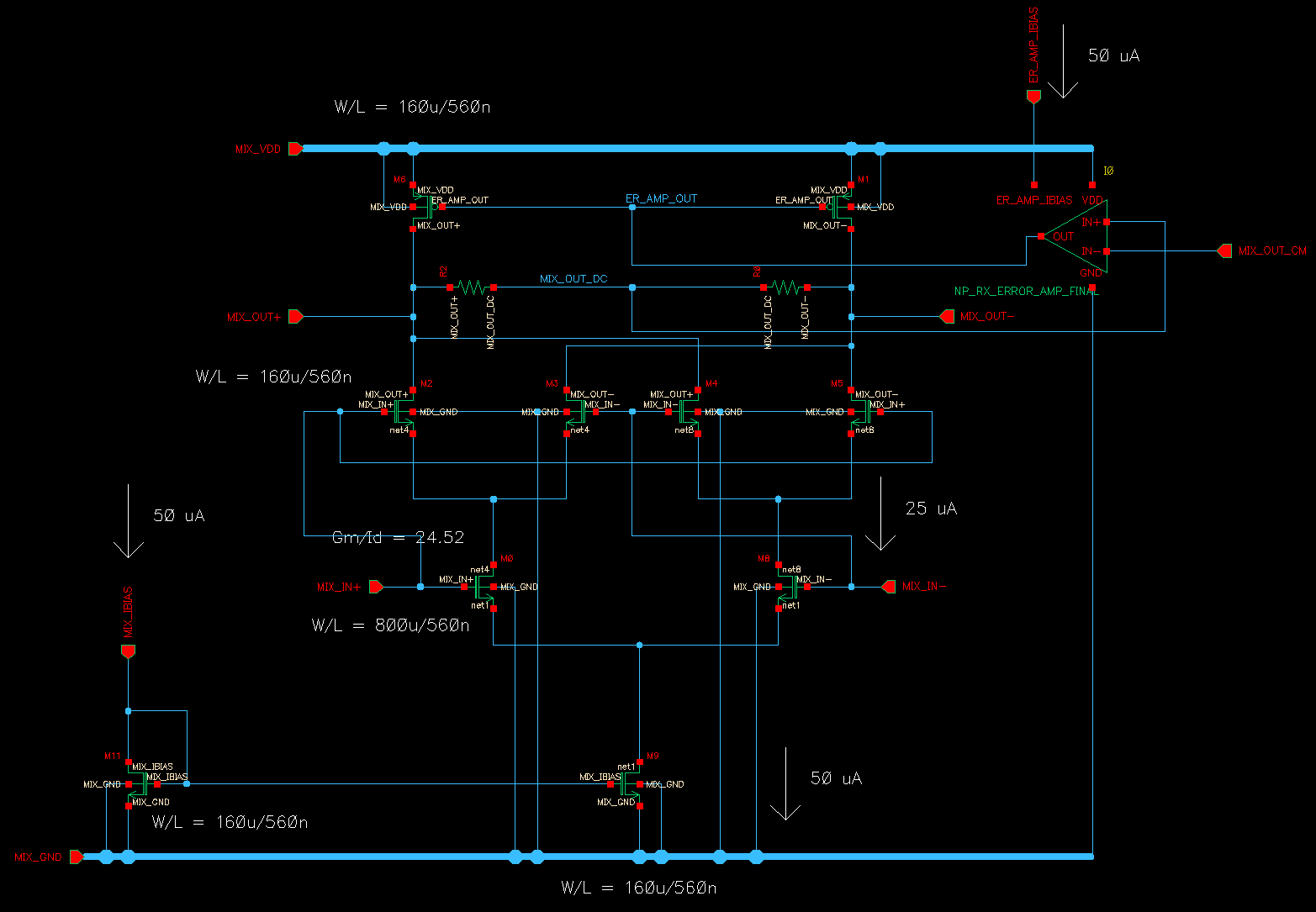
Figure 6. Gilbert Cell Mixer schematic.
We implemented a Gilbert Cell based mixer where LO+ and RF_IN+ are shorted and similarity, LO- and RF_IN- are shorted as shown in the figure. We implemented a common mode feedback (CMFB) loop to set the mixer output DC level. Having control over this DC level is important to avoid false detection by comparators. Since we have control over the mixer output CM and comparator threshold voltage, we can control the tradeoff between false detection and no detection (even when an object is present). Error amplifier in CMFB loop is a simple high BW low gain amplifier, where low load impedance is achieved by diode configured PMOS load.
The mixer consumes 200uA current (100uA + 100uA bias) at 2.5 V supply. Gm/Id of 24.52 was achieved for NMOS transconductors. PMOS load for the mixer gave higher gain which increased sensitivity as now small 40 KHz signals at PGA can also be detected. PMOS load also helped to set output common mode voltage via CMFB loop as explained earlier.
Comparator
We designed a hysteresis comparator to detect the presence of the received signal as shown in figure below

Figure 7. Hysteresis comparator schematic.
As shown in the figure above, M22-M21 form the input of the comparator M23,M24 form the internal positive feedback required to latch. If βM23/ βM25 or βM24/ βM21 >1 hysteresis will occur as positive feedback will be reinforced. M13-M16 form the current mirror pair for providing a DC bias current. The outputs of the comparator are connected to skewed inverters(M2-M3) and (M1-M0) which drive the subsequent stages. The DC bias current for the comparator is 50µA. The input common mode voltage was 1.5V. Figure 8 shows the simulated hysteresis characteristics for different process corners. There is no significant degradation with respect to process corners. The nominal input hysteresis range is 0.8V. The comparator reference voltage can be adjusted externally through a potentiometer.
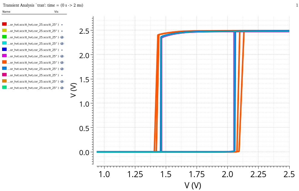
Figure 8. Hysteresis plot of the comparator.