
Counter Logic and SPI Interface
Counter Logic
The counter logic will count the temporal difference between transmitted pulse and the received signal. In order to prevent false alarms, it is essential to ensure that the received signal is at least 8 pulses long. Figure 1 below shows the counter logic. We have two counters. The comparator output is connected to a 5 bit counter (counter_2) which detects if the received signal is at least 8 pulses long. This activates the counter_1 which is a 12-bit counter. The 12 bit counter starts incrementing as soon as the transmitter sends a pulse. It stops incrementing once counter_2 confirms that the received signal is at least 8 pulses long. Counter_1 also generates a READY signal which tells the FPGA to read the counter value. As shown in Figure 2, the counter an edge detector detects the rising edge of the comparator output. This is then buffered and then fed into the 5-bit counter. If 8 or more pulses are seen, the second most MSB will be high, which will indicate counter_1 to stop incrementing. Figure 3 below shows the timing diagram of the counter logic. Each counter itself is ripple counter consisting of D flip-flops. The counter logic can also be reset externally from the FPGA.
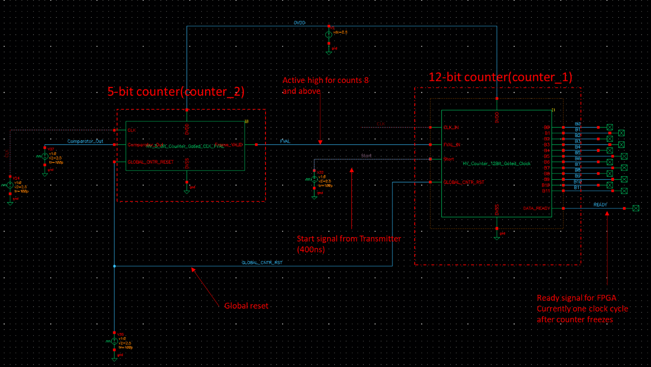
Figure 1. Counter block diagram.

Figure 2. Counter logic.

Figure 3. Counter logic timing diagram.
SPI Interface
The transmitter is controlled from an FPGA through a serial-peripheral interface (SPI) interface. The SPI block being used was provided to us by the course TAs. The SPI block was originally created through synthesis and was based on 1V logic. We therefore added level shifters, hysteresis invertors and buffers to up or down convert from 2.5V to 1V and vice-versa. Figure 4 is a schematic of a 1V to 2.5V level shifter. Figure 5 shows the schematic of the hysteresis inverter.
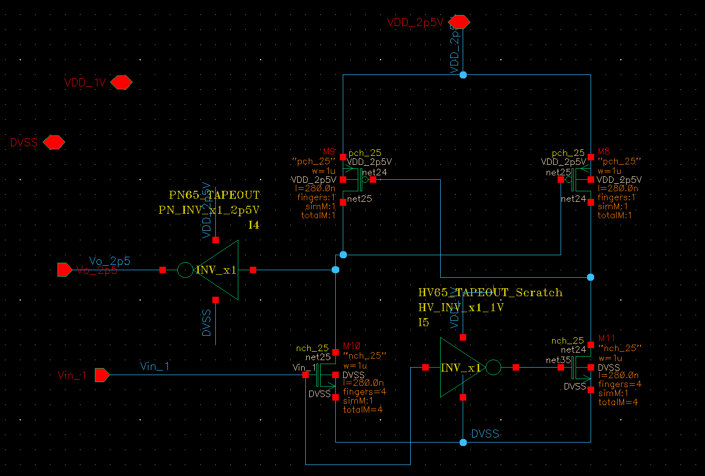
Figure 4. 1-to-2.5V level shifter.
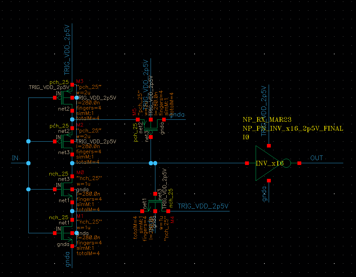
Figure 5. Hysteresis buffer schematic.