
System Overview
Compared to conventional amplifiers (Class A/B) that operate as linear devices, class D audio amplifiers can be understood as switching amplifiers. The power device (MOSFET) acts like a switch, changing its state between off and on by a pulsed signal. This allows for very high efficiencies, up to 90 - 95%.
The basic principle of class D amplifier is shown in Figure 1: input the audio signal into the comparator, and compare it with the triangle wave signal to obtain the PWM signal, meaning that the input is encoded as the duty cycle of the pulse signal. The PWM signal and its opposite, then drive an H-bridge, turn on and off power devices to create an AC signal to the speaker, in between a filter circuit is required.
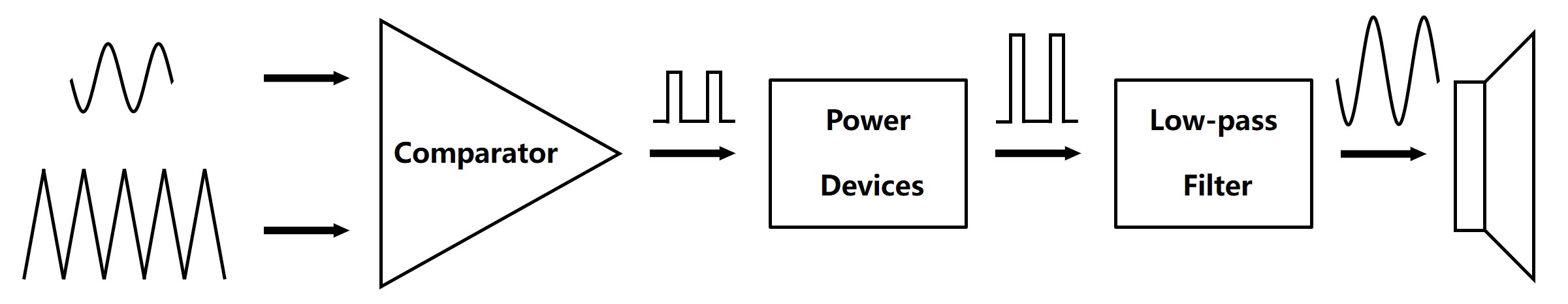
Figure 1: Basic principle of class D amplifier
Figure 2 shows the process of pulse width modulation using a comparator. At the positive peak of the sine wave, the duty cycle of the rectangular pulse is close to 100%, and at the negative peak it is close to 0%. Here, the frequency of the triangle wave signal needs to be much higher than the maximum frequency of the audio signal. (at least 10 times higher than the upper limit of human hearing of 20KHz)
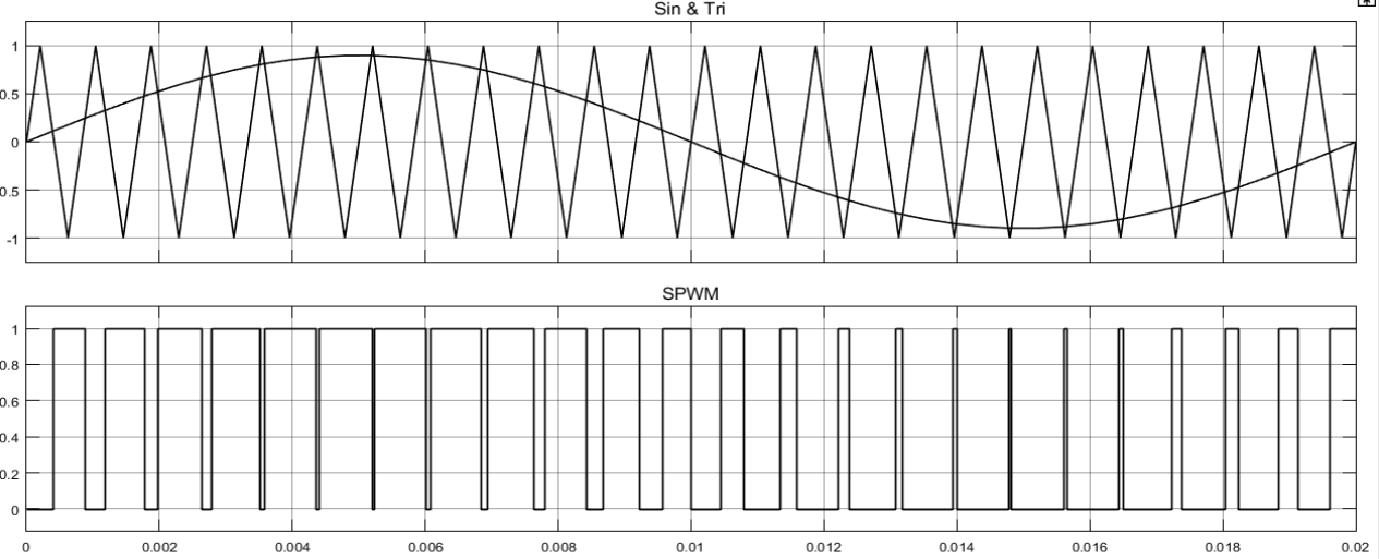
Figure 2: Pulse Width Modulation
In our class D audio amplifier, as shown in Figure 3 and 4. the first block in the signal chain is the single-ended to differential converter. It takes two inputs INL and INR, sums them up, and converts to differential. The VREF is at 1.25V to provide common mode voltages for all the operational amplifiers. Two more reference voltages are required, TRIH at 1.9V and TRIL at 0.6V. These two voltages set the voltage range for the relaxation oscillator which generates the triangle wave.
The overall system is a feedback amplifier with a gain set by the 100k and the 200k resistor. The 10pF capacitor is a compensation capacitor that sets the first pole of the amplifier at roughly 50kHz to stabilize the loop. The 22pF capacitors set the dead time for the gate drive signals.
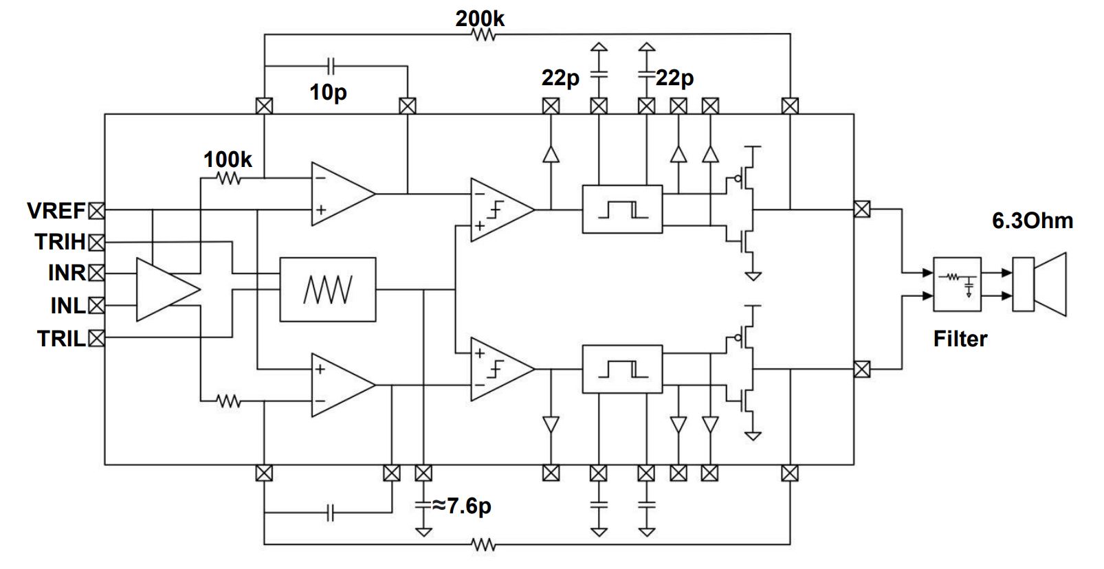
Figure 3: System Block Diagram
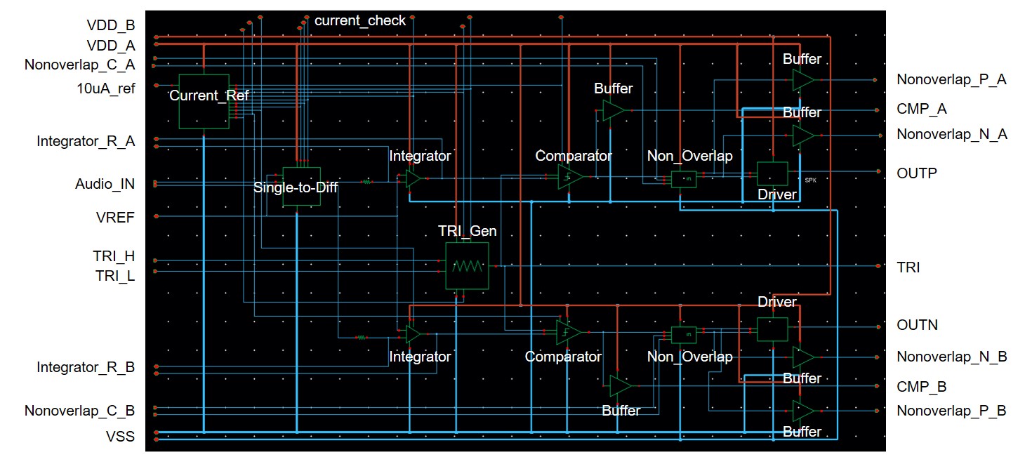
Figure 4: Schematic Diagram
Based on this structure, table 1 shows our design specifications.
| VDD | 2.5V | Max Output | ±2.3V @ 8 Ohm |
| FTRI | 500kHz | Max Input | ±0.575V |
| Bandwidth | 49kHz | PSRR | >72dB |
| Efficiency | 94% | Deadtime | 60nS | ROUT | 500 mOhm | HD3 | 1% |
Table 1: Design Specifications