
Introduction
Welcome to the Class D Amplifier home page of this Project with an introduction.
The goal of this project was to design and fabricate a single channel high efficiency and low distortion class D audio amplifier in a 65nm foundry CMOS process.
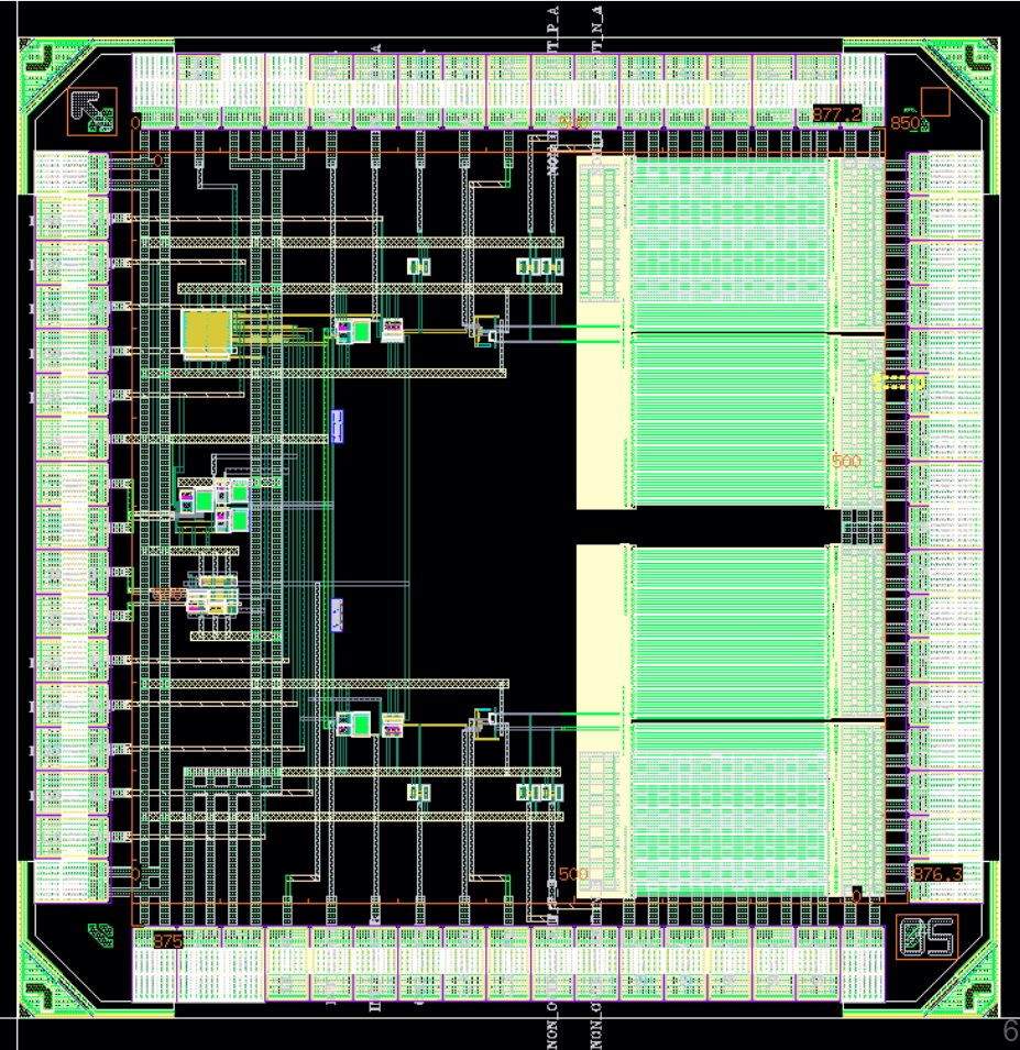
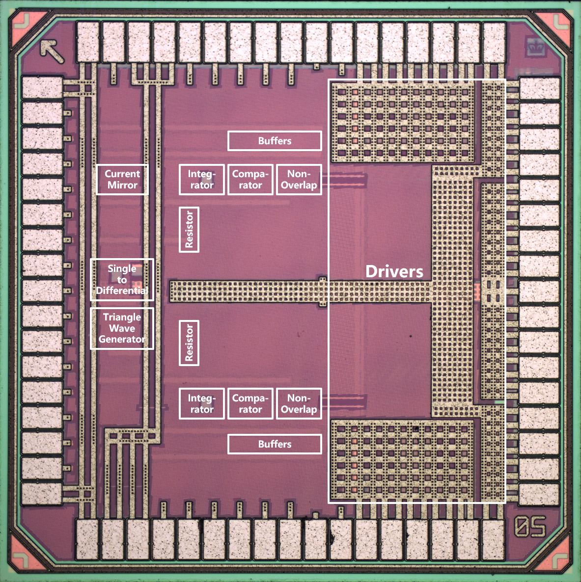
The class D audio amplifier was designed on an 1 mm2 area using 2.5V IO devices. The input audio from a smartphone is converted to differential on-chip. The differential signal is fed through two single-ended paths each consisting of an error amplifier, a comparator, a dead time generator, a gate driver, and finally an output bridge. The modulation scheme was a pulse width modulation (PWM), achieved by comparing the sine wave signal with a 500kHz triangle wave signal.
The design achieves 0.082% (-61.7dB) HD2, 1.43% (-56.9dB) HD3 at 1kHz, 1Vrms output level driving an 8 Ohm speaker. The quiescent current of the design is 4mA. The efficiency is up to 93.3% at maximum output.
 |
|
| Figure 1: GDS Stream of the Class D Amplifier | Figure 2: Die Shot of the Class D Amplifier |