Block Design
In this section, the simulation results of the chip are introduced.
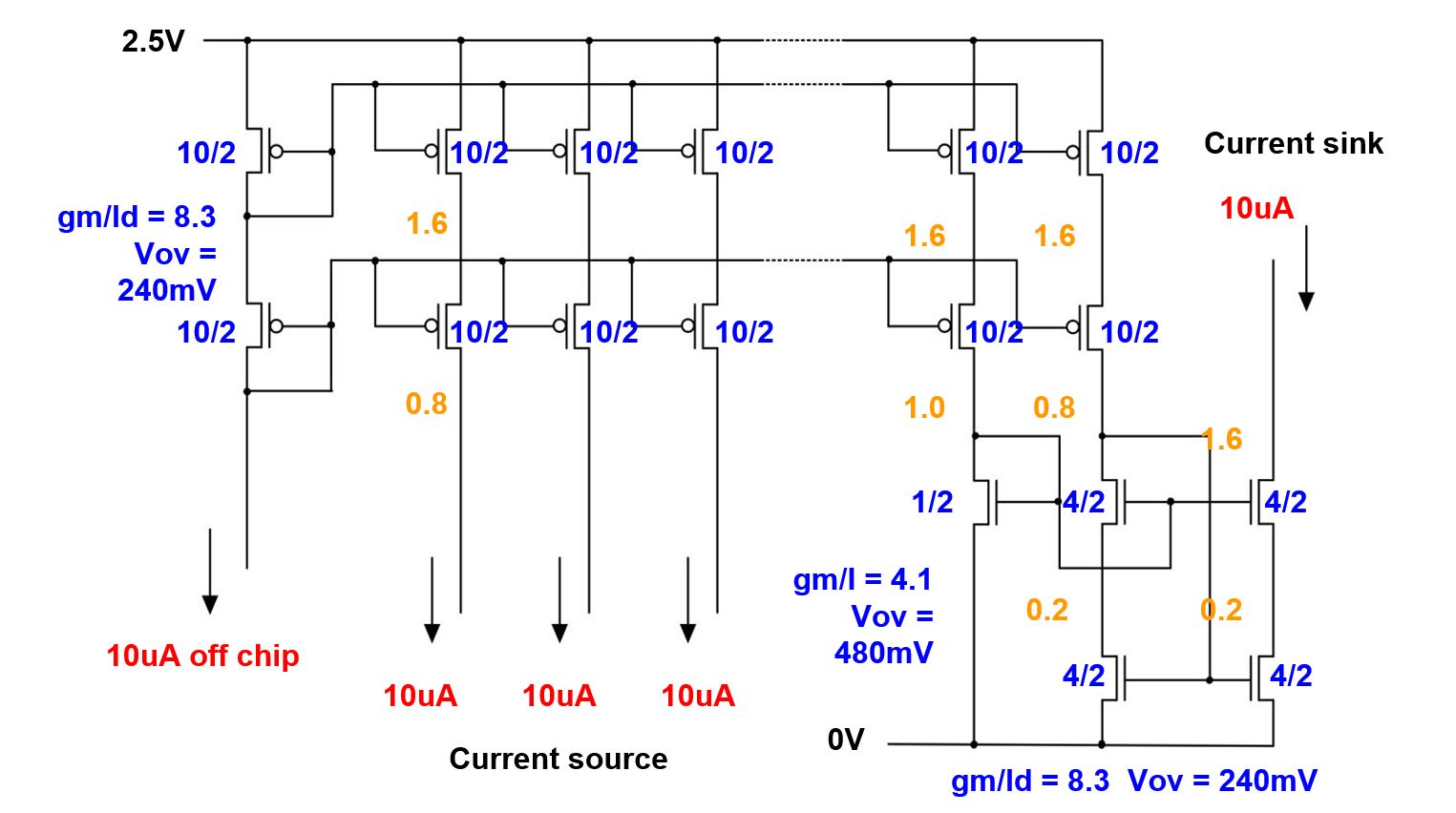
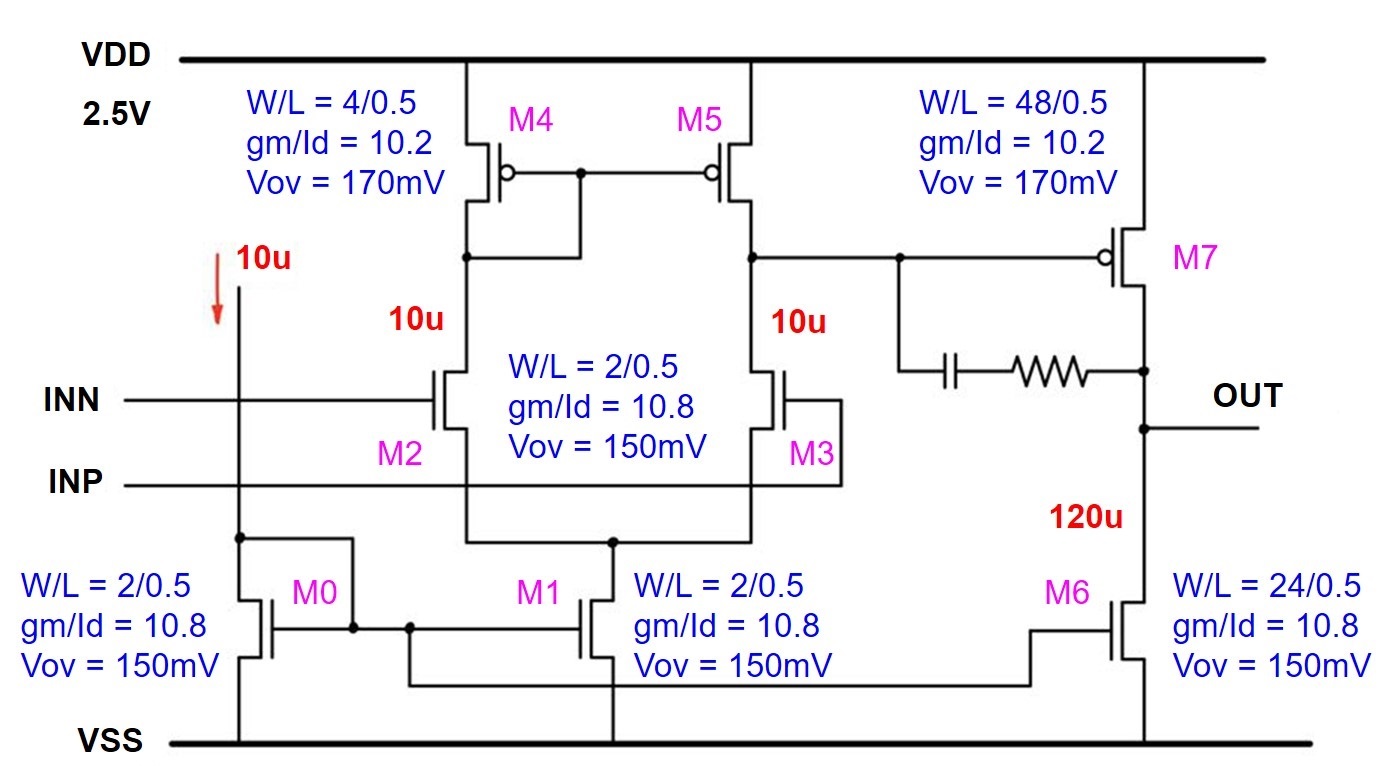
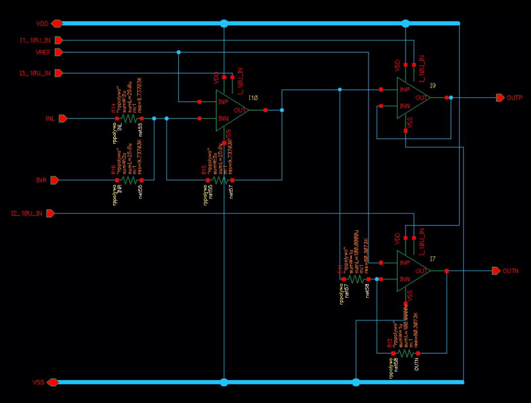
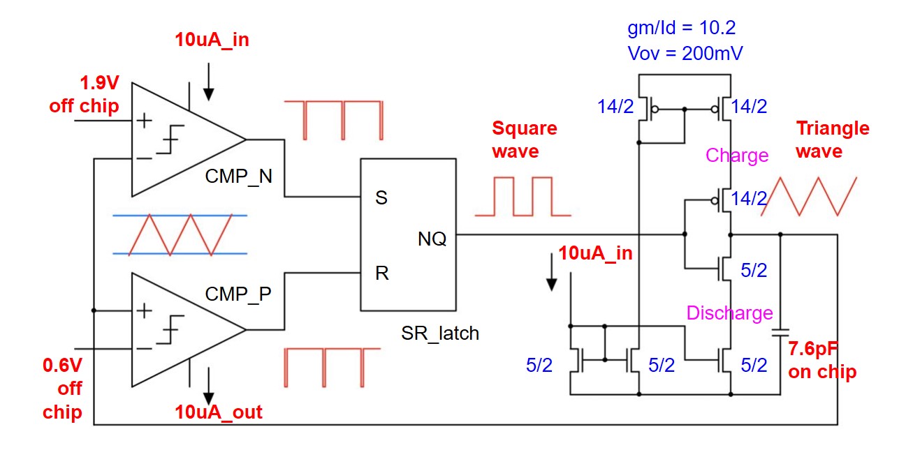
Figure 1: Miller OTA Figure 2: Single-ended to Differential Converter Figure 3: Block_design_3_Tri_gen Figure 4: NMOS Input Comparator Figure 5: PMOS Input Comparator Figure 6: Non-overlap Clock Generator Figure 7: Cascode Current Mirror
Figure 1 shows the two-stage Miller OTA with miller compensation, which is used as the error amplifier. It has a gain of 75dB, a phase margin of 80 degrees, and a GBW of 33MHz. The same block is also used to build the single-ended to the differential converter, as shown in Figure 2.
The 500kHz triangle wave is generated by a relaxation oscillator, as shown in Figure 3. The load capacitor is charged and discharged with constant current 10uA to generate positive and negative ramps. The comparators and the SR Latch generate the square wave to switch between charging and discharging for the load capacitor.
Two different comparators were designed for the triangle wave generator. This is because the two operate at different common mode levels (0.6V and 1.9V). The NMOS input pairs are good at a high CM level and the PMOS input pairs are good at a low CM level. These comparators are also used in further pulse width modulation.

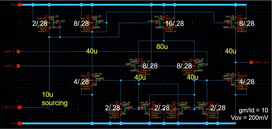
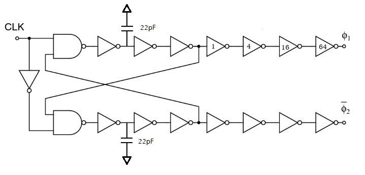
Figure 6 shows the non-overlapping clock generator that drives the output stage is implemented using an SR latch with a delay in its feedback path. The delay is implemented with a series of inverters and an additional load capacitor off-chip to adjust the dead time. This significantly increases the rise time at the node of the capacitor which increases the jitter of the clocks.
The current biasing of all circuits, as shown in Figure 7, was implemented using cascode current mirrors with off-chip reference.