
PCB design
The schematic and layout of PCB are shown here.
Figure 1 and 2 shows the block diagram of all the components on the PCB.
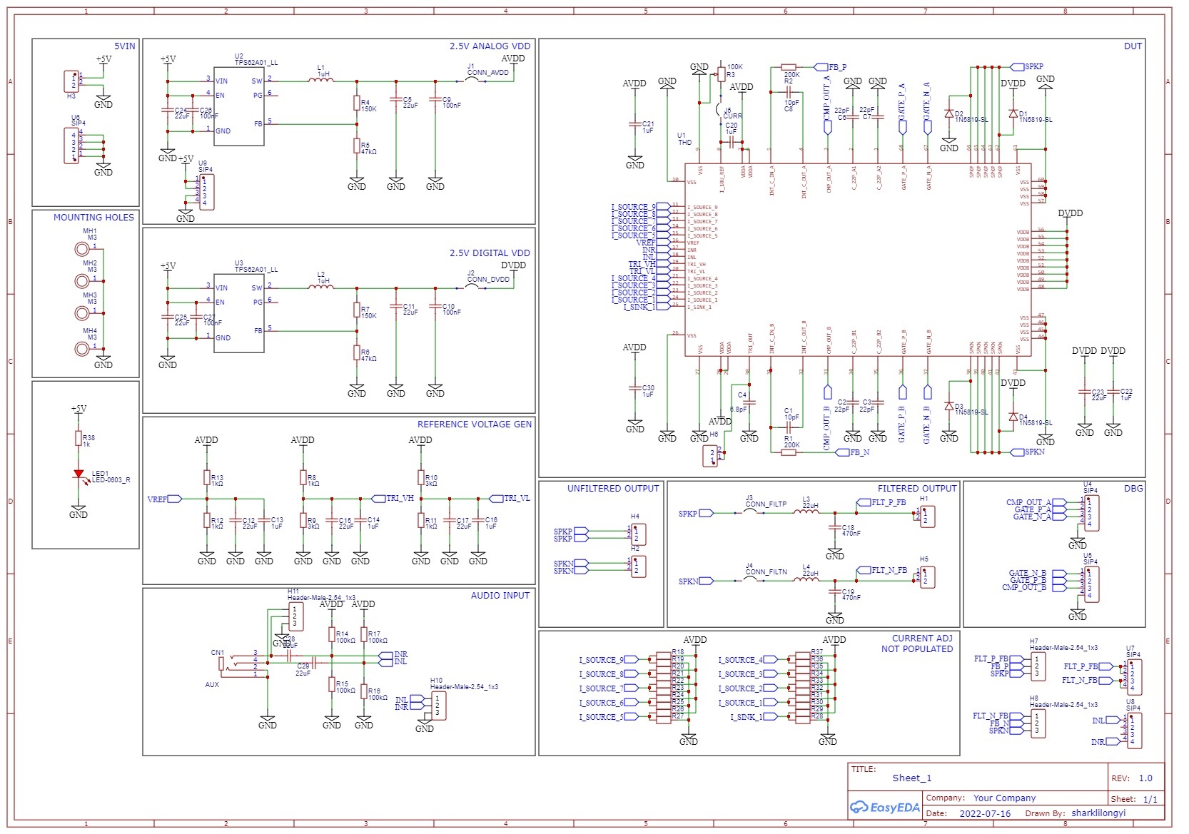
Figure 1: Schematic of PCB
The chip is placed in the center and the connection to the speaker is added on the right side. There are two voltage regulators, one for AVDD and one for DVDD.
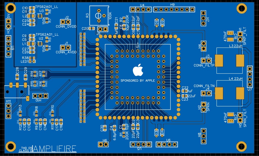
Figure 2: Layout of PCB
The figure below shows the complete PCB, populated with all components. A 4.5V battery is used for the power supply of the chip.
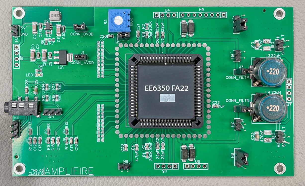
Figure 3: PCB Assembly
A 4-inch 2-way bookshelf seaker is driven by the class-D amplifier, powered by 3 AAA Batteries in series.
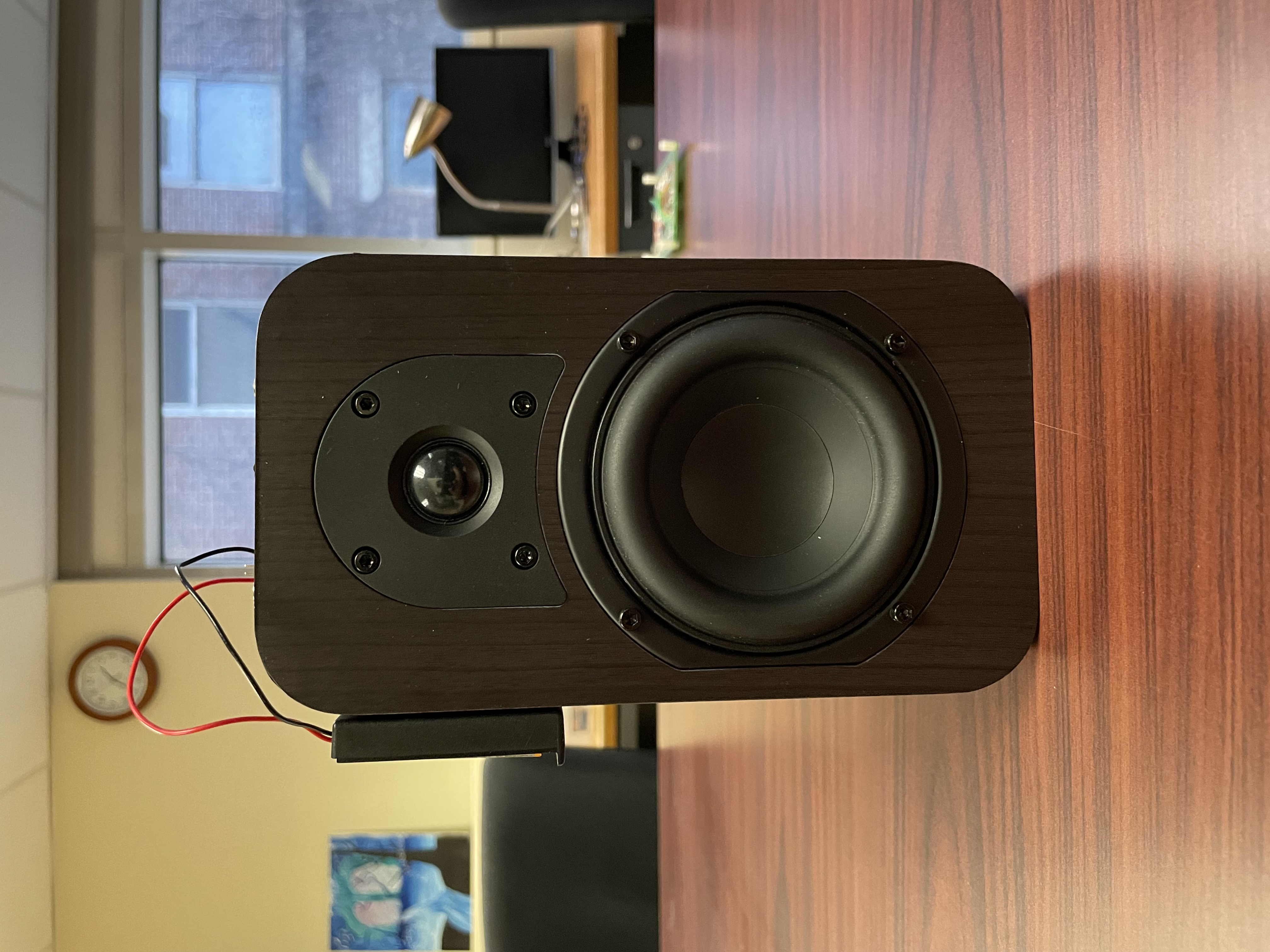
Figure 4: Portable Speaker
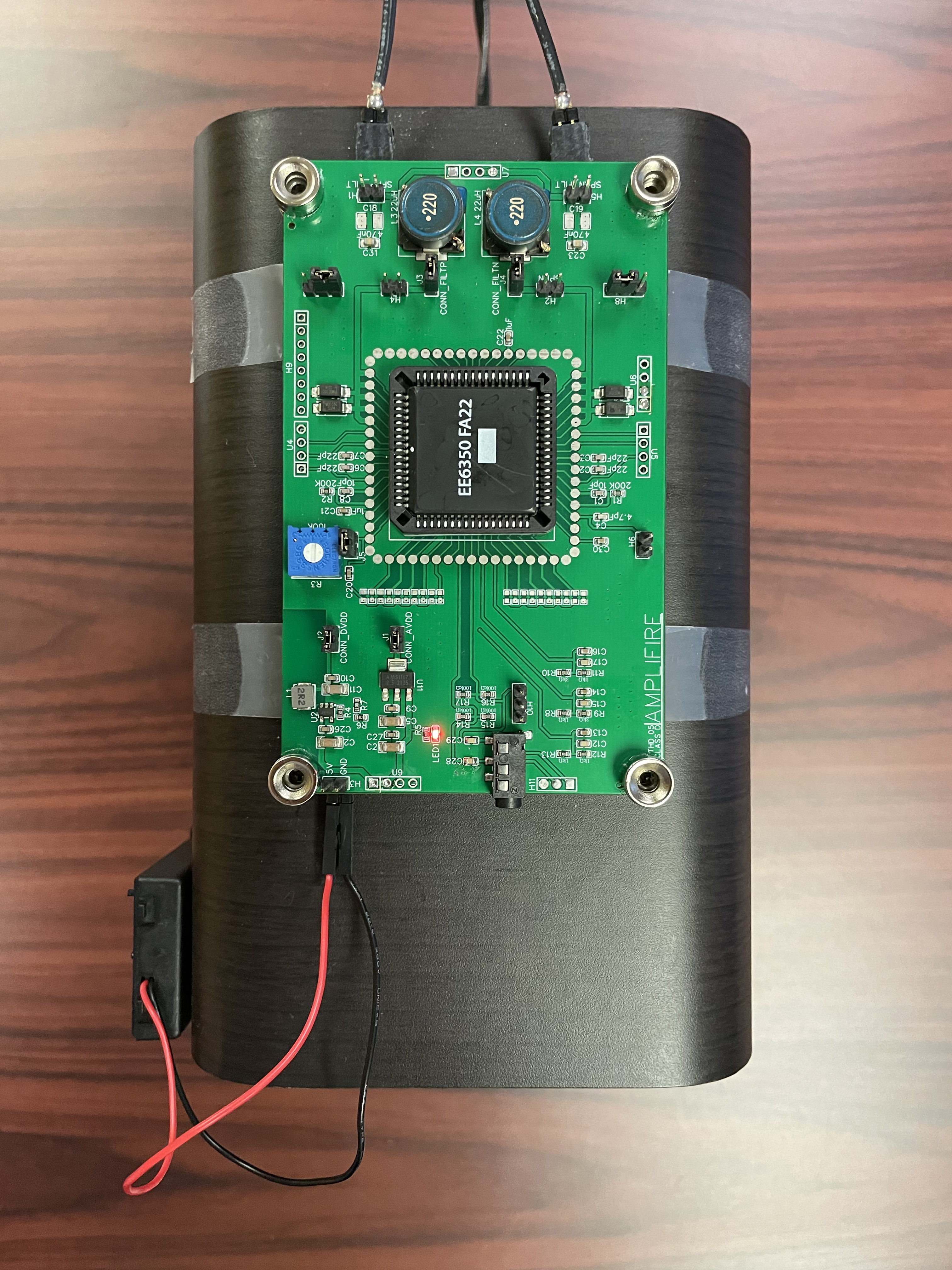
Figure 5: Portable Speaker