Layout
In this section, the layout of the whole chip and each building block in the chip are shown.
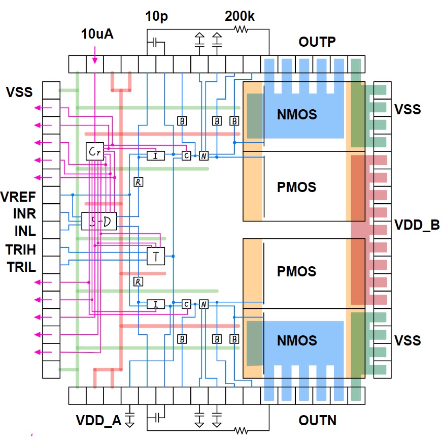
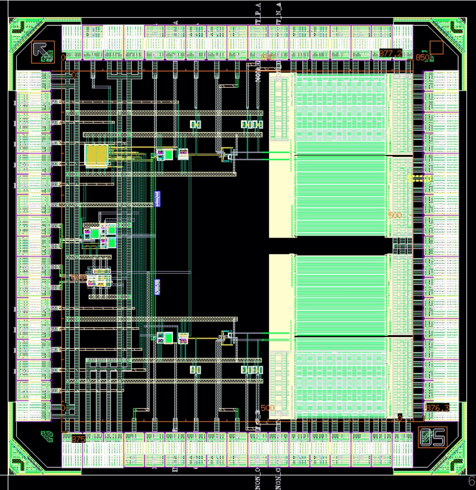
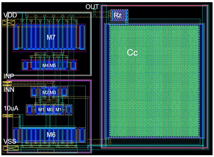
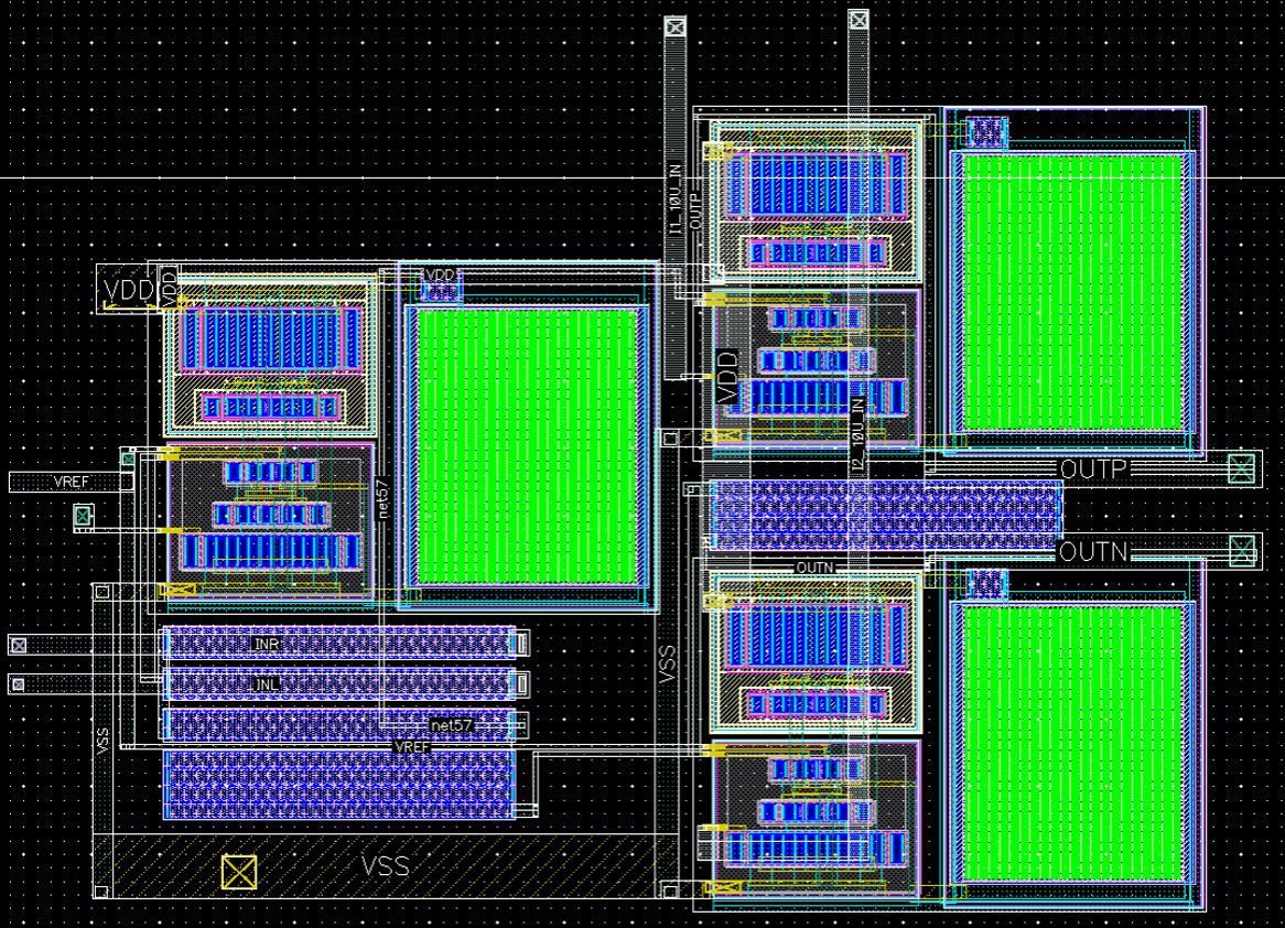
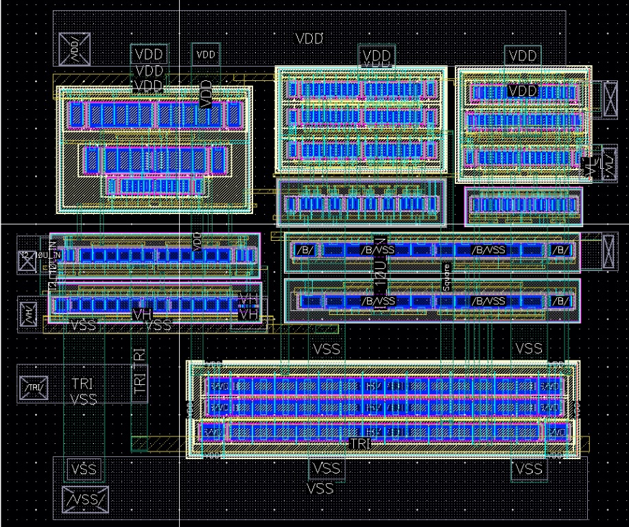
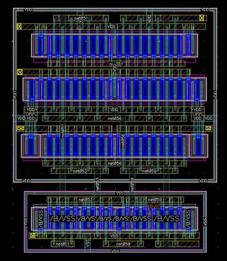
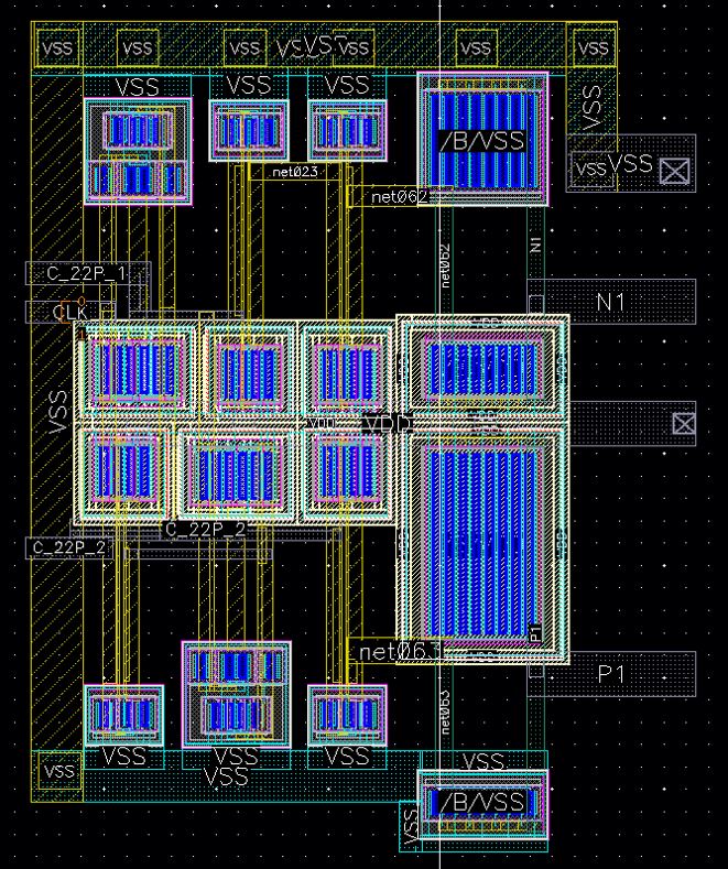
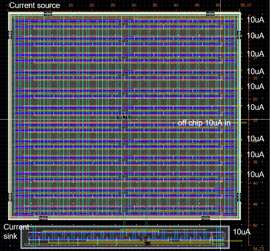
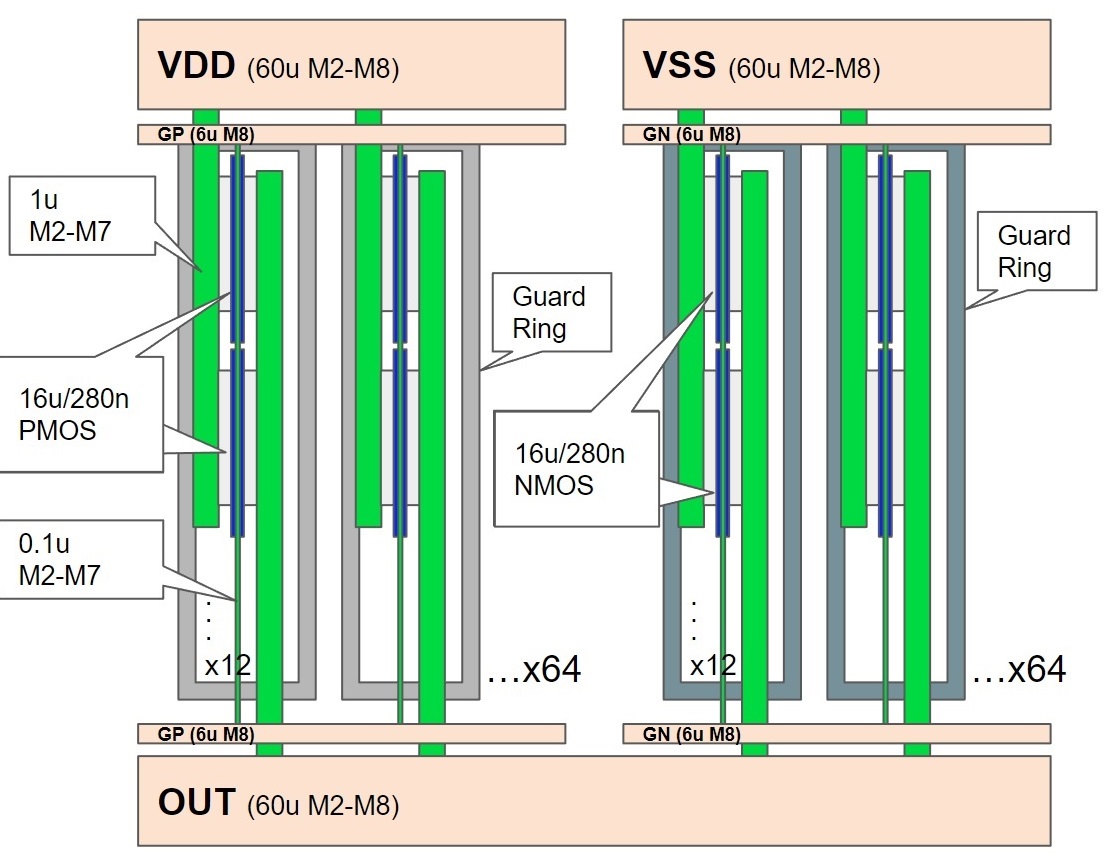
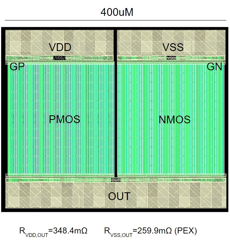
Figure 1: Chip Floorplan Figure 2: Chip Layout Figure 3: Miller OTA Layout Figure 4: Single-ended to Differential Converter Layout Figure 5: Triangle Wave Generator Layout Figure 6: NMOS Input Comparator Layout Figure 7: PMOS Input Comparator Layout Figure 8: Non-overlap Clock Generator layout Figure 9: Cascode Current Mirror Layout Figure 10: Output Driver Floorplan Figure 11: Output Driver Layout
Figure 1 and 2 show the floorplan and whole layout for the chip.