
Implementing a GaN Output Stage For More Power Output
The power output of the amplifier is mainly limited by the supply voltage of the output devices. At 2.5V, the maximum power a 8 Ohm speaker can dissipate is less than 1W. To increase the power output, an external H-Bridge with a higher supply voltage can be used.
Gallium nitride (GaN) is a III/V semiconductor material that is better suited for power applications compared to silicon because of a lower RDSon and a lower gate capacitance meaning they can switch faster. Therefore, a GaN output stage EPC2152 was selected due to its availibility. The device features a 80V 15A GaN half bridge with integrated gate drivers capable of 3MHz maximum switching speed. Two of these devices were used at 12V to make an H-bridge to drive the speakers.Figure 1 shows the original block diagram
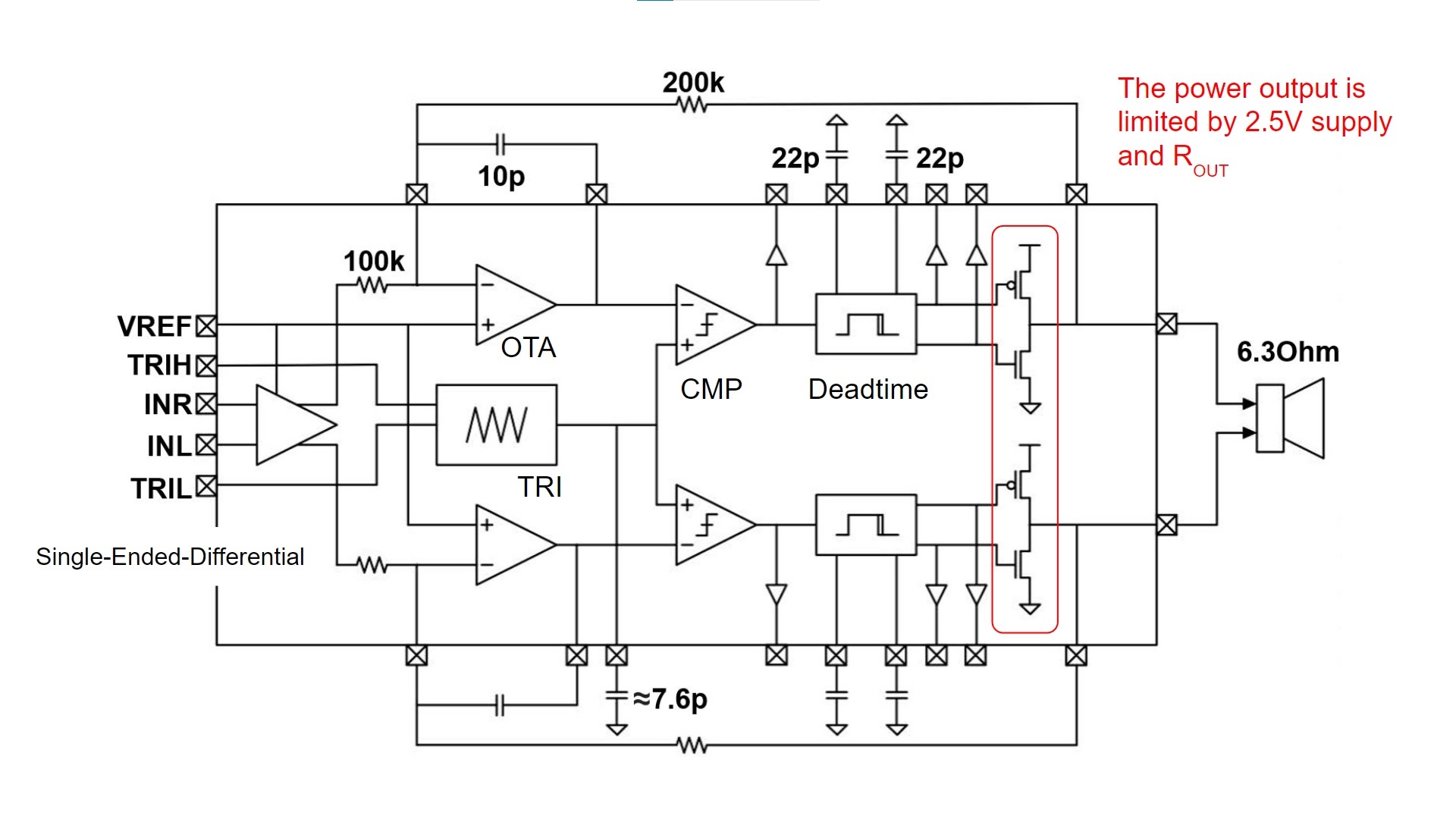
Figure 1: Original Block Diagram
Figure 2 shows the modified block diagram with the GaN half-bridge
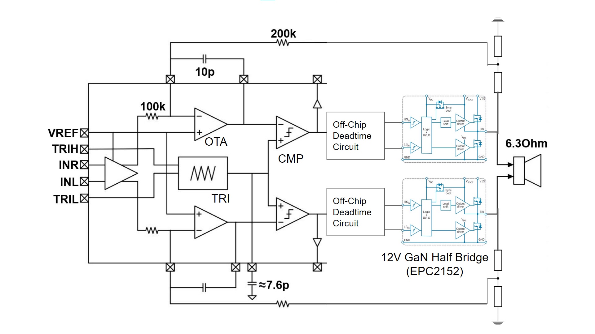
Figure 2: Modified Block Diagram
The figure below shows the PCB design. New deadtime circuits are required. This is because the original deadtime circuit on chip is loaded by the Cgs of the output stage on chip which creates more delay. The new deadtime circuits also provides level shifting from 2.5V to 3.3V.
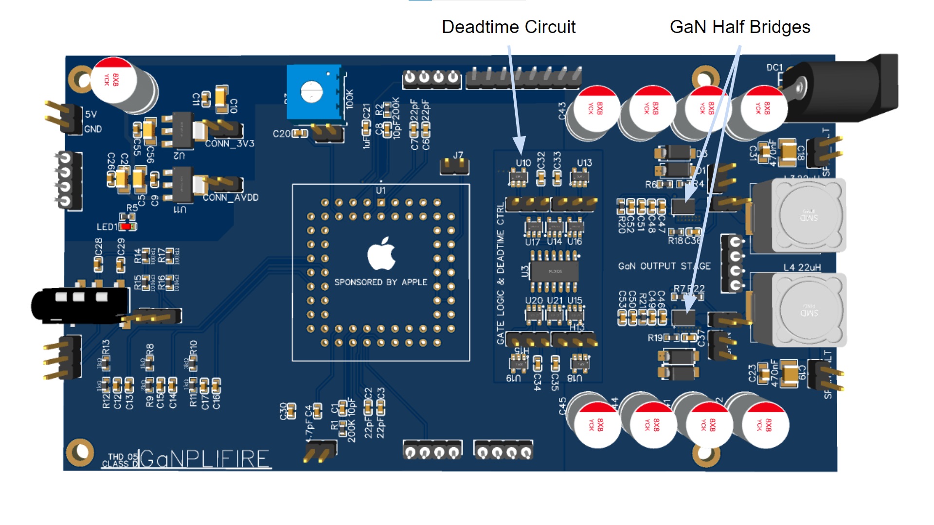
Figure 3: PCB Design
The new design requires a 12V DC supply from an AC/DC adapter.
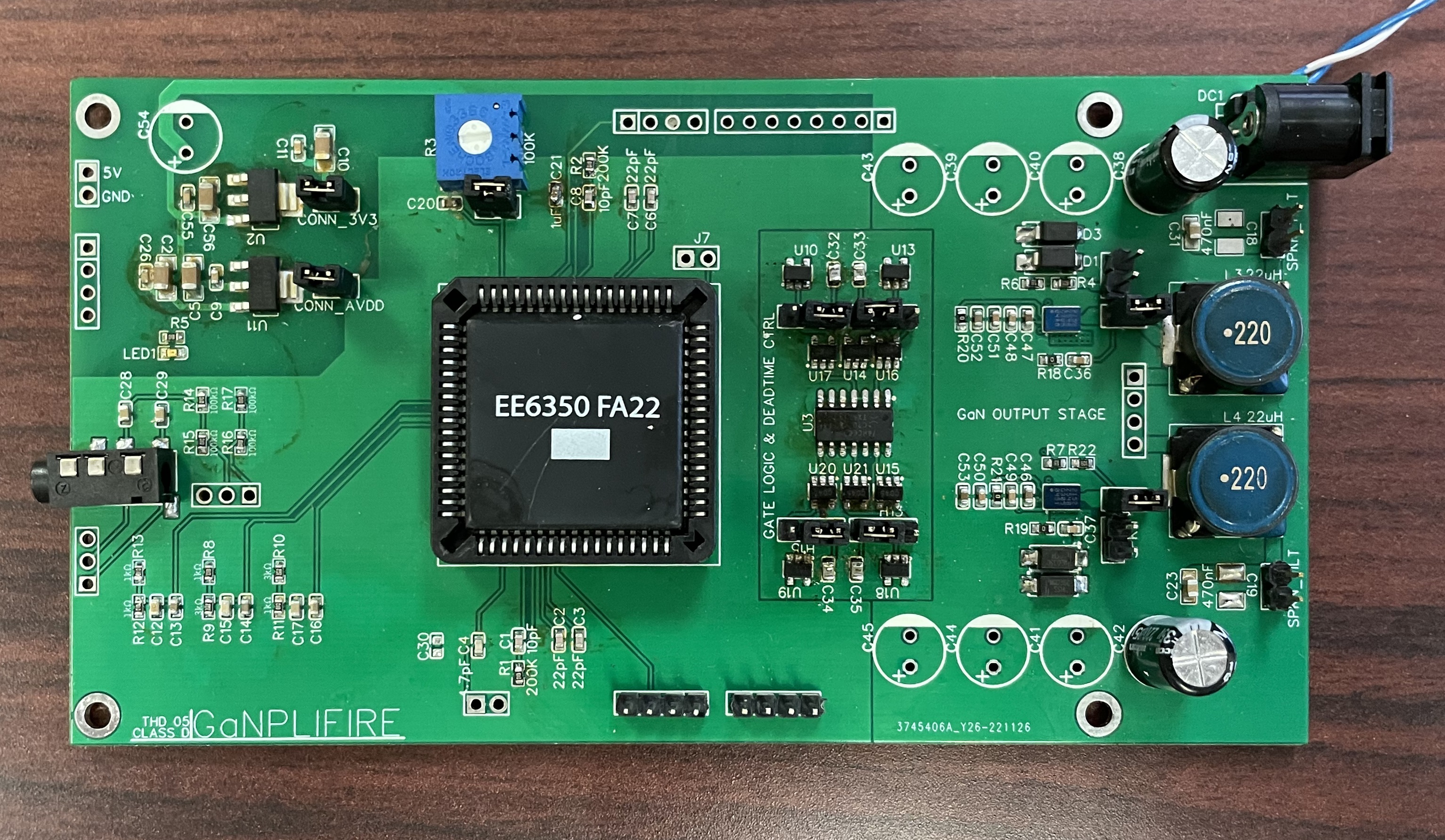
Figure 4: GaN PCBA