
Introduction
Welcome to the home page of the Digital Clock chip project. Please navigate through the website to get to know more about this project.
This project is part of the courseVLSI Design Lab (EE6350), taught by Prof. Peter Kinget in Spring 2022 at Columbia University. This course is mainly focusing on exposing students to the entire IC design flow, so that students can learn more practical skills and knowledge through the tape-out experience.
This project is made possible by the generous contribution from Apple Inc, who sponsored the fabrication and package of our chip.
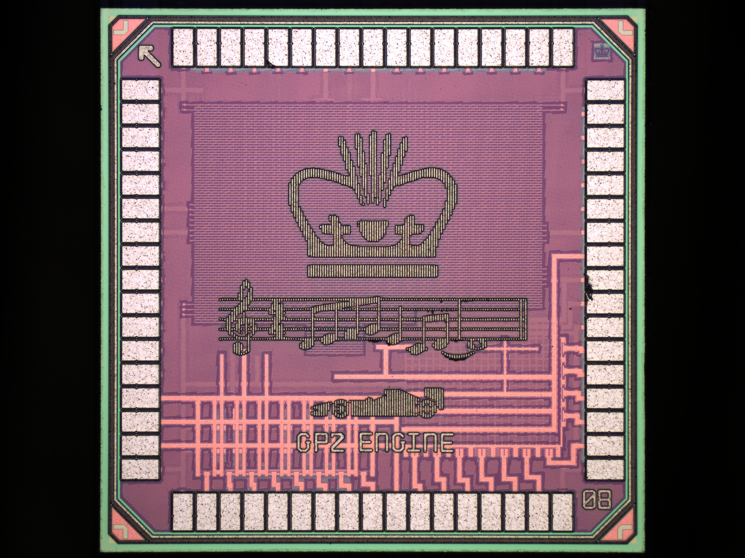
Fig. 1: Die Photo
This project is completed by a team of 4 students. Our team converted an idea into a full GDS, in a custom design approach. We designed the schematic, and then converted it to layout. The silicon is manufactured in TSMC 65 nm technology. A PCB system was built to demonstrate the functionalities of the chip. You can find all the details in this website.