
IC Layout
Block Layout
We manually layout the chip in Cadence Virtuoso, and verify the layout with Calibre DRC/LVS/PEX.
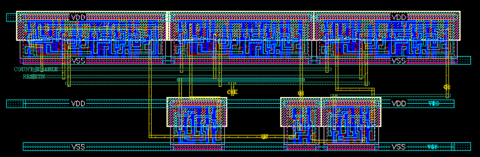
Fig. 1: Modulo 8 Block Layout
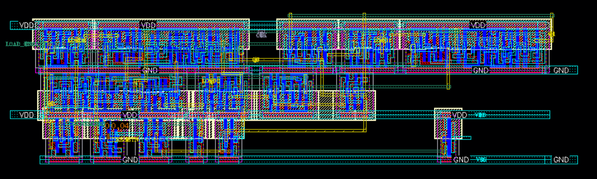
Fig. 2: Modulo 6 Block Layout
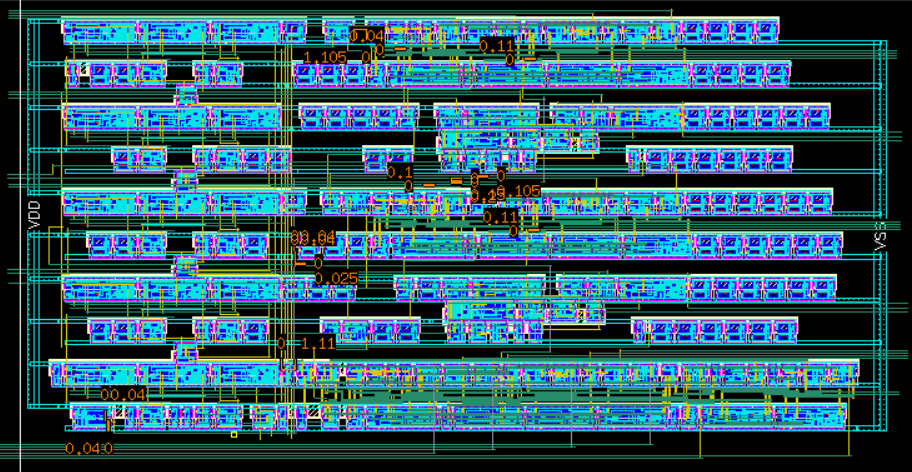
Fig. 3: Clock Counter Layout
Chip Floorplan
Chip floor plan is shown on Fig. 4.
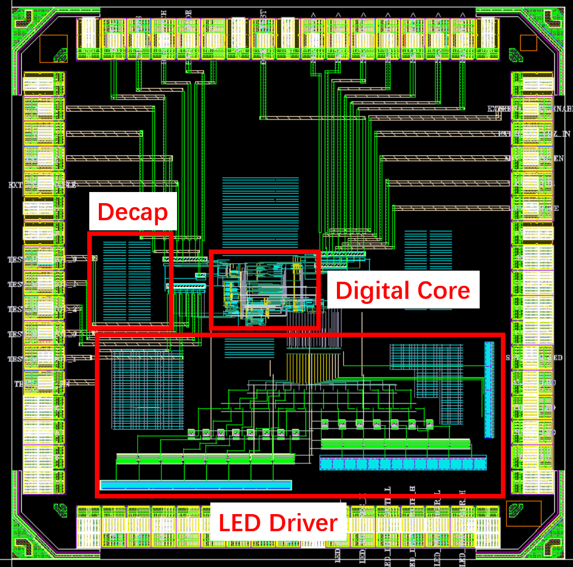
Fig. 4: Floor Plan
Clock Distribution
We used clock tree to reduce clock skew. Each branch is buffered.
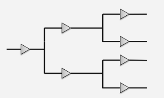
Fig. 5: Clock Tree Illustration
Power Distribution
We used power grid to distribute power to reduce power IR drop. To further improve power stability against logic switching, we also added decoupling capacitors near each block. Decap will shorten the current return patt, which reduce L·dI/dt drop.