
IC Design
Clock Timer Alarm Button Input Driver Block Verification
Clock
1. Clock Counter Overview
Counter module basically is just counters. We firstly use a 32768 counter to convert 32.768kHz clock signal into a 1Hz square wave (50% duty cycle). This 1Hz signal will be fed into clock counters, to be hours, minutes and seconds.
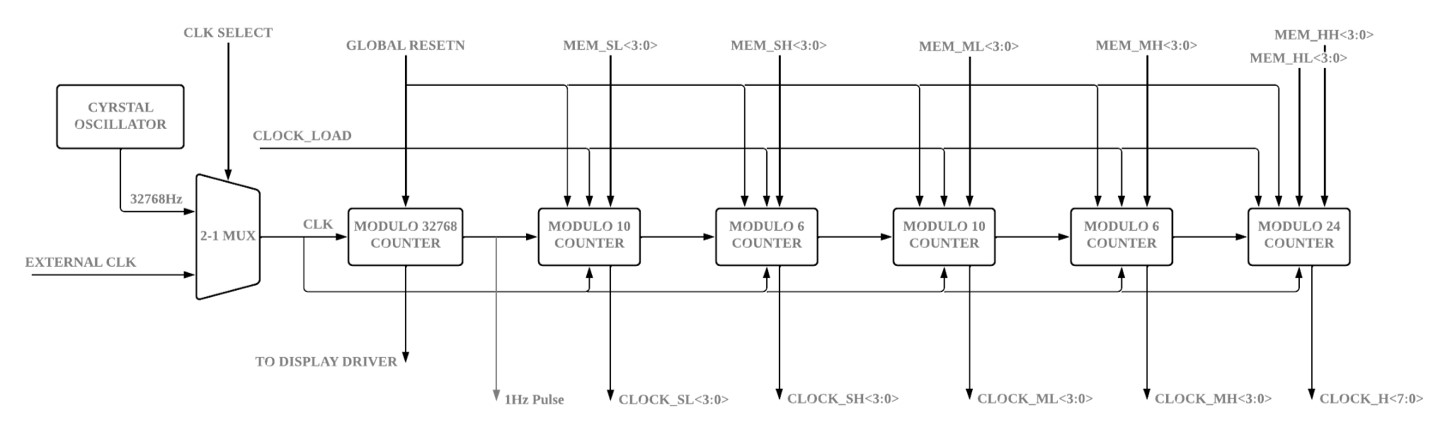
Fig. 1: Clock Counter Diagram
2. Modulo 32768 Counter
Because of 32768 = 215, we can convert it to a 50% duty cycle square wave with a 15-bit synchronous counter. A typical synchronous counter is built by toggle flip-flop and and-gate. We put five 3-bit counter in series here, to avoid 15-bit and-gate for typical 15-bit synchronous counter. The 3-bit counter is shown in Fig. 2 and Fig. 3. We used Cadence Virtuoso to design and simulate our circuits. To reduce the design workload, we used standard cells in most blocks.
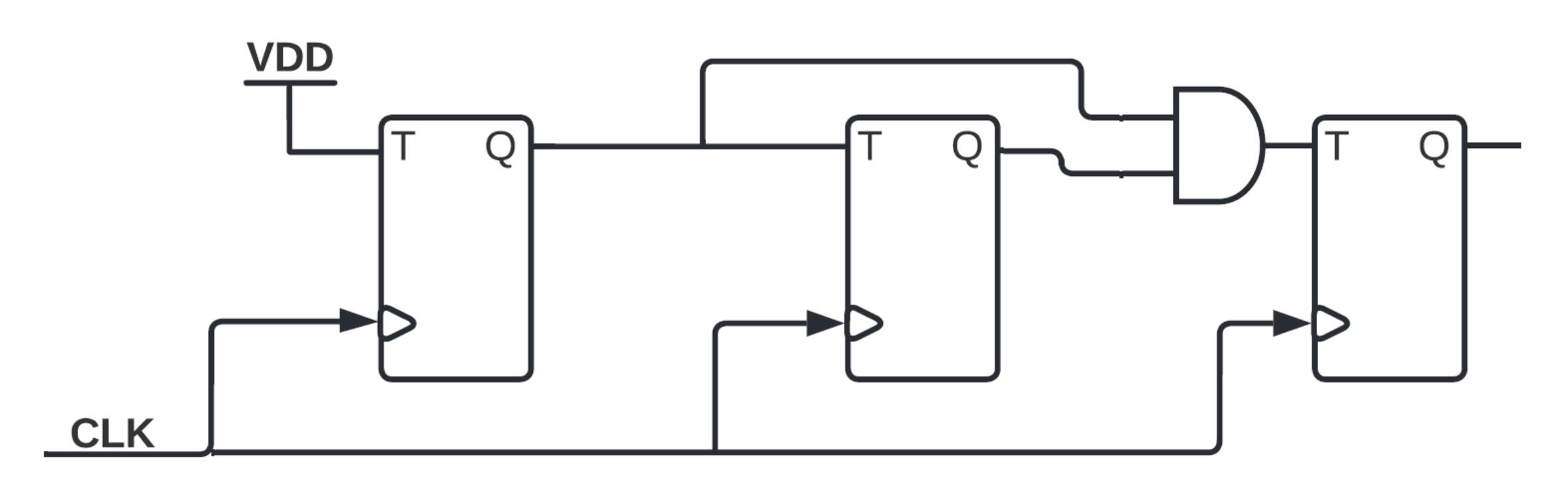
Fig. 2: 3-bit Synchronous Counter (Modulo 8)
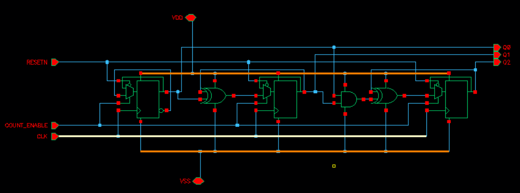
Fig. 3: 3-bit Synchronous Counter (Modulo 8)
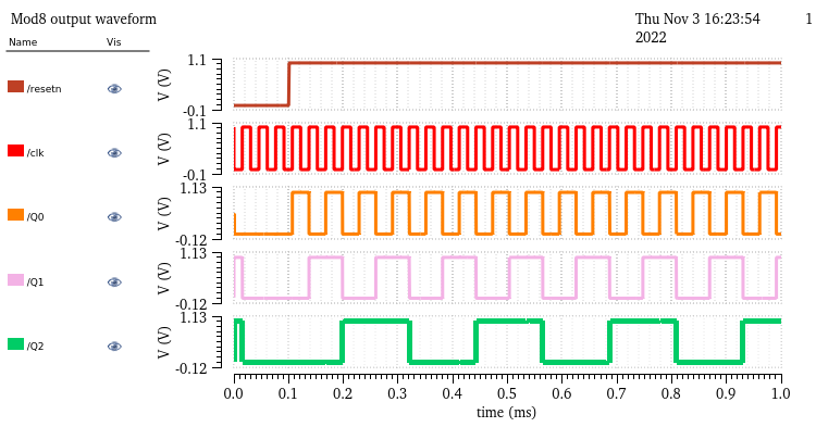
Fig. 4: Modulo 8 Simulation Waveform (Output in BCD)
3. Modulo 10 Counter
Modulo 10 Counter counts from 0 to 9, which is 0000 to 1001 in binary. In this case, we cannot use the simple counter architecture because we need to reset after reaching 1001. An additional block is added here to reset the counter to avoid overflow.
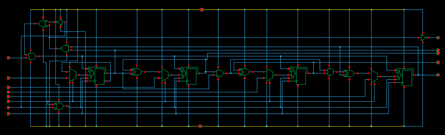
Fig. 5: Modulo 10 Counter
Timer
The design of timer is similar to clock counter. The difference is that timer use down counter instead of up counter in clock.
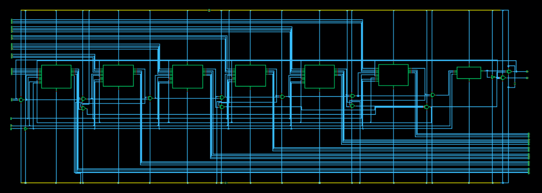
Fig. 6: Timer
Alarm
Alarm is made of a comparator and memory. The basic operation is comparing stored time against current clock time. If the stored time si the same as current time, this module will send a signal to start the buzzer.
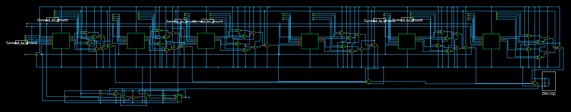
Fig. 7: Alarm
Button Input
Button input is debounced on PCB to achieve a clean waveform. We converted a button signal into a pulse, so that logic block can easily process this signal.
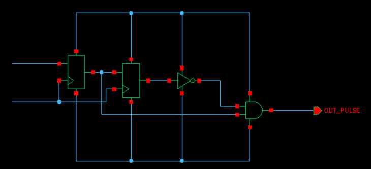
Fig. 8: Pulse Generator
Driver Block
1. Level Shifter
Driver block works in 2.5V domain, but all control signals and data are in 1V. We need to convert 1V siganl into 2.5V. A differential cascode voltage switch logic (DCVS) level shifter is used here. Because it's a ratioed logic, there are contentions in the circuit. A proper trasistor sizing is crucial to make it work. As shown in the figure, drive strength of M1 and M2 should be much weaker than M0 and M3.
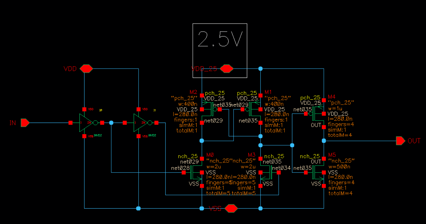
Fig. 9: DCVS Level Shifter
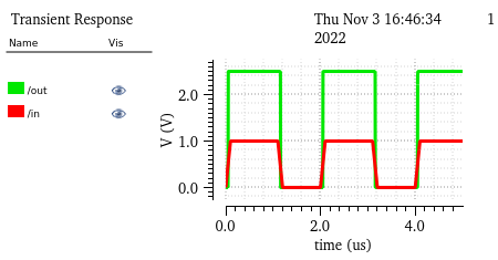
Fig. 10: Level Shifter Waveform (Red: 1V Input; Green: 2.5V Output)
2. LED Display
In order to reduce the chip pins for LED display, we reuse the LED segment enable pins by sweeping 6 digits. The sweeping frequency is 32.768 kHz, and the LED works perfectly at this frequency, without any noticeable blinking. Binary coded time is decoded into 7-segment code and send to driver.
3. Driver
The driver consists of segment enable (PMOS) and digit enable (NMOS). A larger trasistor width is required to conduct large current of LED and buzzer.
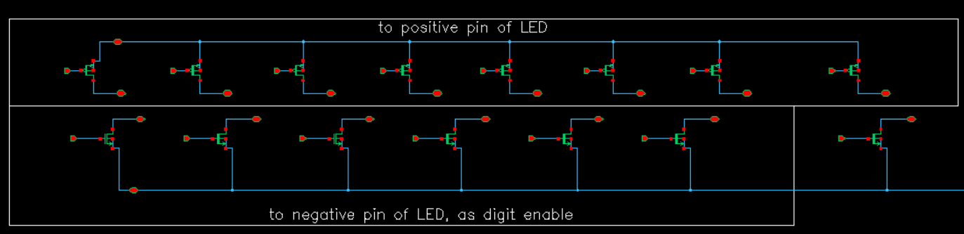
Fig. 11: Driver Schematic
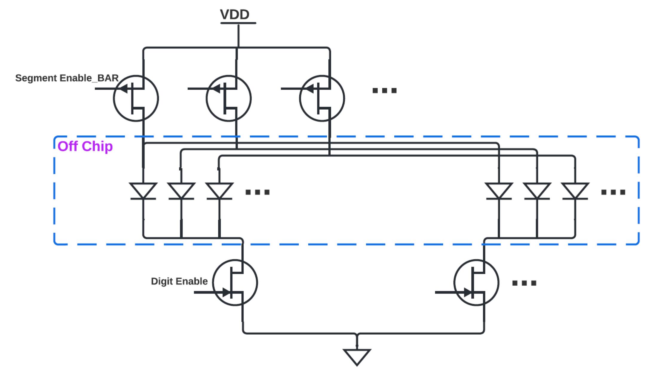
Fig. 12: Driver Diagram
Verfication
Each block is verified in Cadence Virtuoso through transistor level simulations. To achieve more accurate results, we also ran simulations after layout extraction for each blocks across 3 major PVT corners:
- TT, 1.0 Vdd, 25oC: typical
- FF, 1.1 Vdd, 0oC: most suceptible to hold time violation
- SS, 0.9 Vdd, 85oC: most suceptible to setup time violation
The simulations are mainly focusing on functionality and timing. Chip level simulations are not feasible due to the excessive computaional power required. Therefore, we convert the schmetic into gate level verilog and run RTL simulations in QuestaSim for verifications.
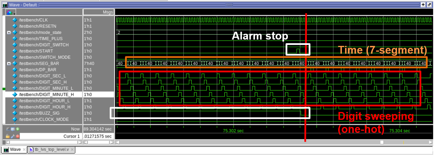
Fig. 13: Gate Level Verilog Simulation