
Schematic Design
Full Chip
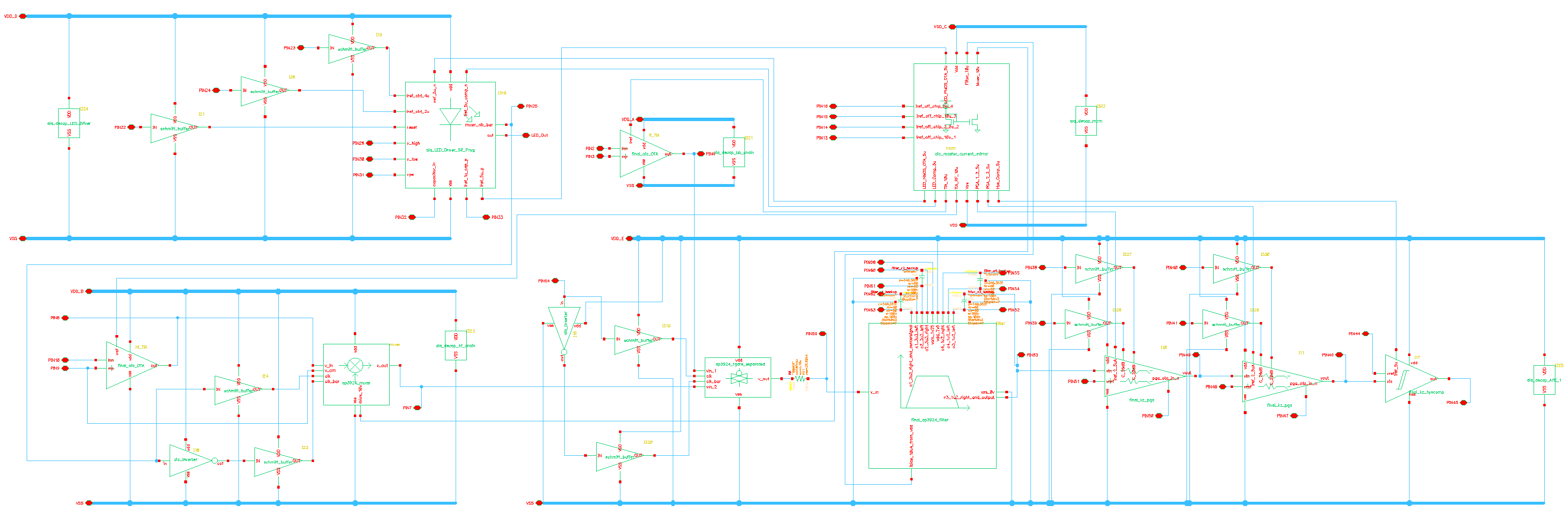
Figure 1. LP-PPG Chip Schematic
The figure above shows the full schematic of the LP-PPG Chip. The chip was divided into five power domains: the LED Driver, the LF chain, the HF chain, the Filter and PGA chain, and the Master Current Mirror. In this section, the design choices and methodologies used to create the individual blocks that make up the chip are explained below.
LED Driver
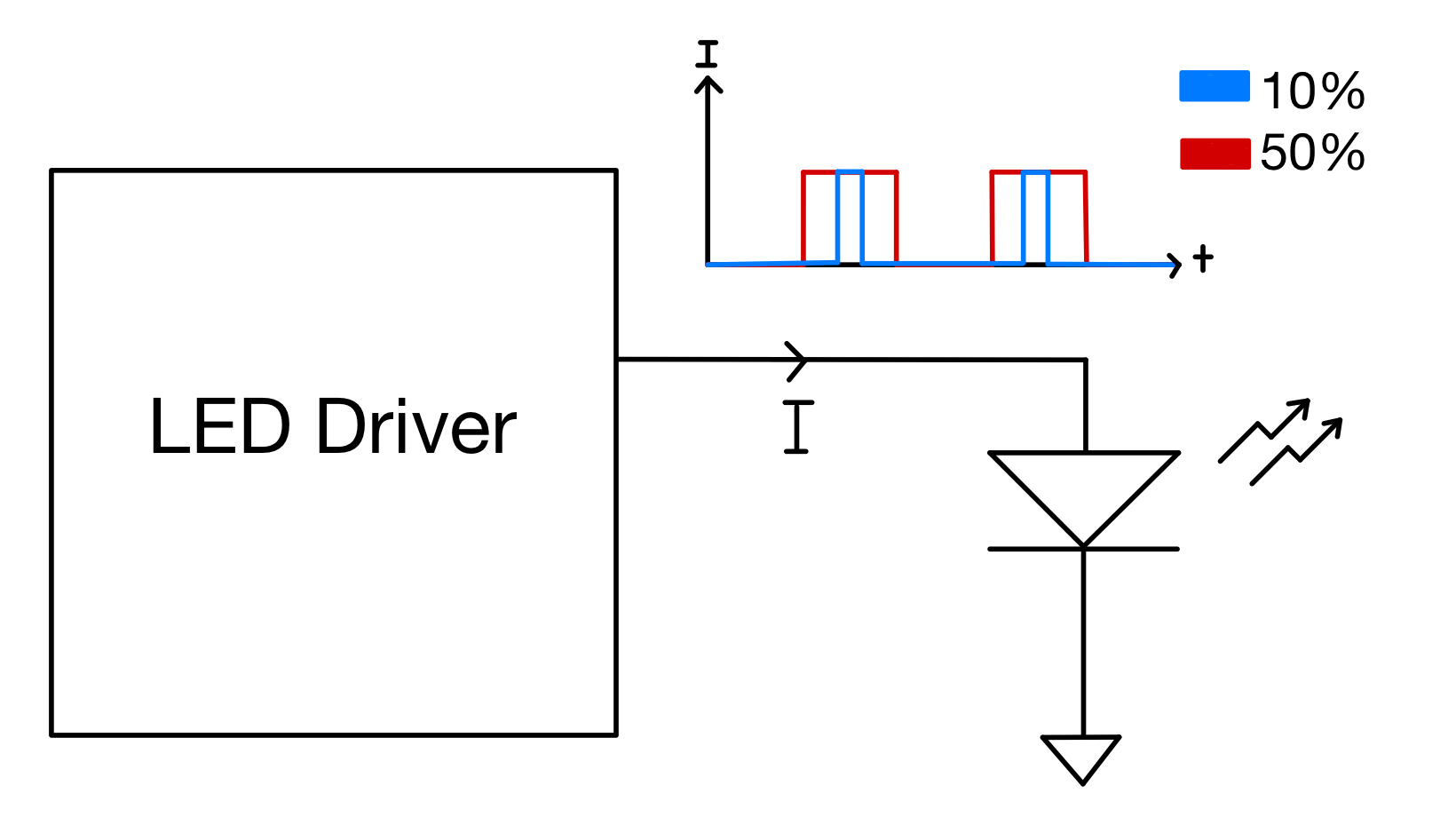
Figure 2. LED Driver Output Signal
The design specification of the LED Driver required that it was able to provide a 100mA low frequency square wave with a variable pulse width to an infrared LED. The oscillator topology that was chosen for this design was a relaxation oscillator. This oscillator works on the function of charging and discharging a capacitor using current to produce a triangle wave. The voltage on that triangle wave is compared using two comparators between two reference voltages. The output of each comparator is fed into an SR Latch, which controls the charging and discharging of the capacitor.
![Relaxation Oscillator Hierarchical View and Waveform [1]](./images/Schematic_Design/Relaxation_Oscillator_Hierarchical_View_and_Waveform.png)
Figure 3. Relaxation Oscillator Hierarchical View and Waveform [1]
To begin the design, a focus was placed on the current being used to charge a capacitor and capacitor’s value. To charge and discharge the capacitor, a current mirror was constructed with PMOS current mirrors for charging and NMOS current mirrors for discharging. The PMOS and NMOS current mirrors were mirrored to one another to provide equal pull up and pull down for the charging of the capacitor to create a 50/50 clock cycle. To size the transistors of the current mirror, a gate length of 3.2um and 1.6um for the PMOS and NMOS respectively was chosen to mitigate the effect of channel length modulation to provide an accurate current between the reference current and the mirrored current. The widths were then chosen to get the transistors into saturation and correspond to the current being mirrored. Additional transistors of 2x the width and 4x the width were added with switches underneath the device to create higher current modes for higher frequencies. The switches were placed below the PMOS transistors in order to ensure good matching of the Vgs between transistors.
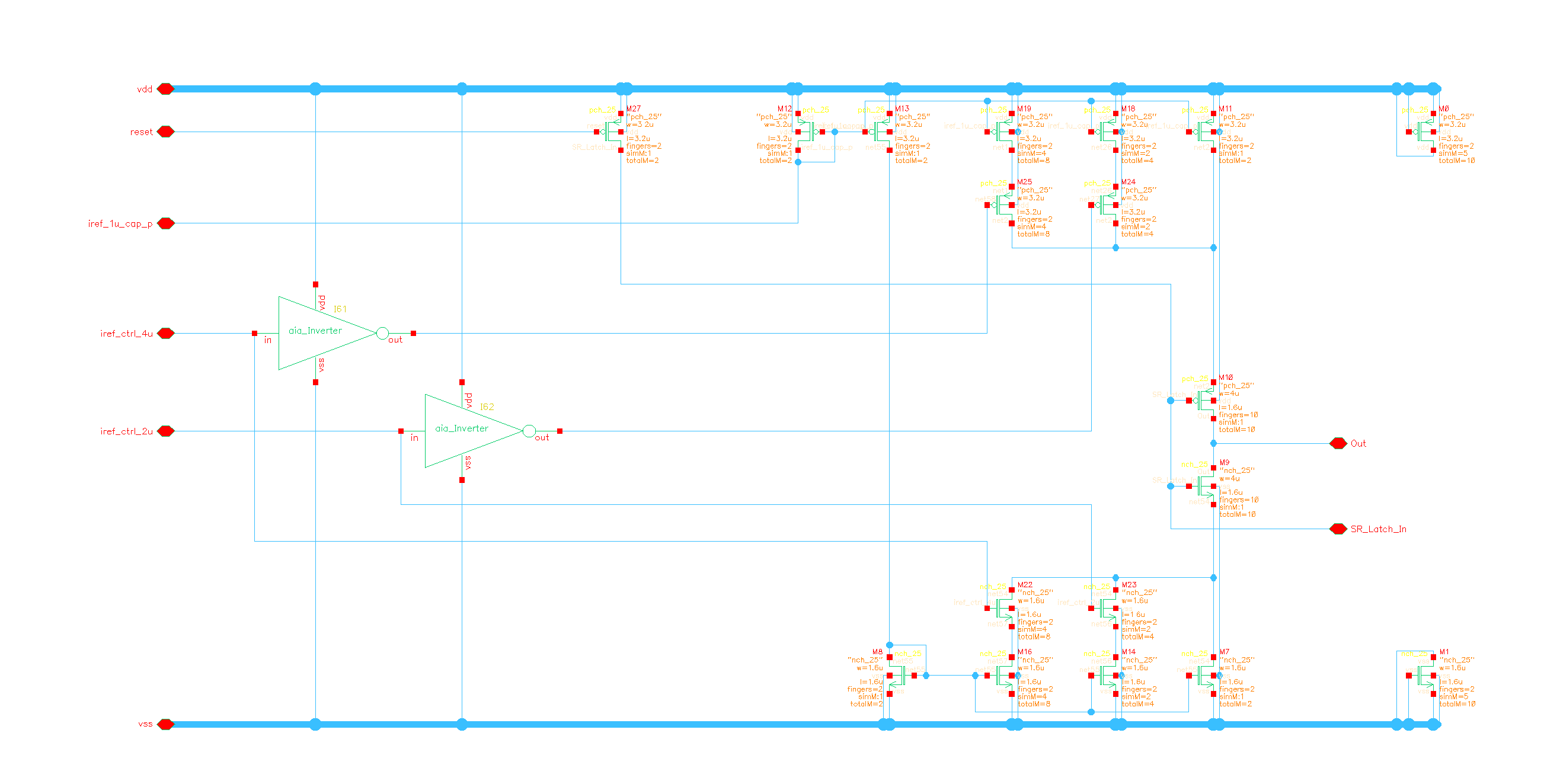
Figure 4. LED Driver Current Mirror
Originally, an on chip MOM-capacitor with a value of 2pF was used. However, due to the frequency range of this oscillator being between 1kHz to 20kHz, this required a current of 1nA to produce a 1kHz wave. The small current would have resulted in a high amount of noise on the current, which would translate into high phase noise on the oscillator's output. It was then decided to use a 1uA current to charge the capacitor, which resulted in a 330pF off-chip capacitor being required.
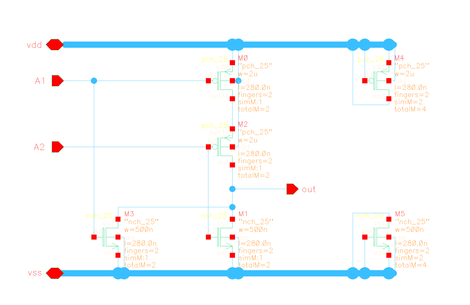
Figure 5. NOR Gate of SR Latch
The design then focused on the comparators and SR Latch used for controlling the charging and discharging of the capacitor. The reference voltages chosen for this design were a V_Low of 0.5V and a V_High of 2V. These voltage references were created using a resistor divider using polysilicon resistors on chip. The resistor values were chosen to be each 55.33kOhm as this reduced the current being dissipated by the resistor divider and allowed for better matching between each resistor. The SR Latch NOR gate was sized using the minimum length and a 2um and 0.5um width for the PMOS and NMOS respectively, to provide a high switching speed. The reason for this sizing was because the control gate of the current mirror was sized to be 40um to get the gate to operate in the subthreshold region, where the leakage of the gate would be minimized as well as minimize the noise on the triangle voltage.
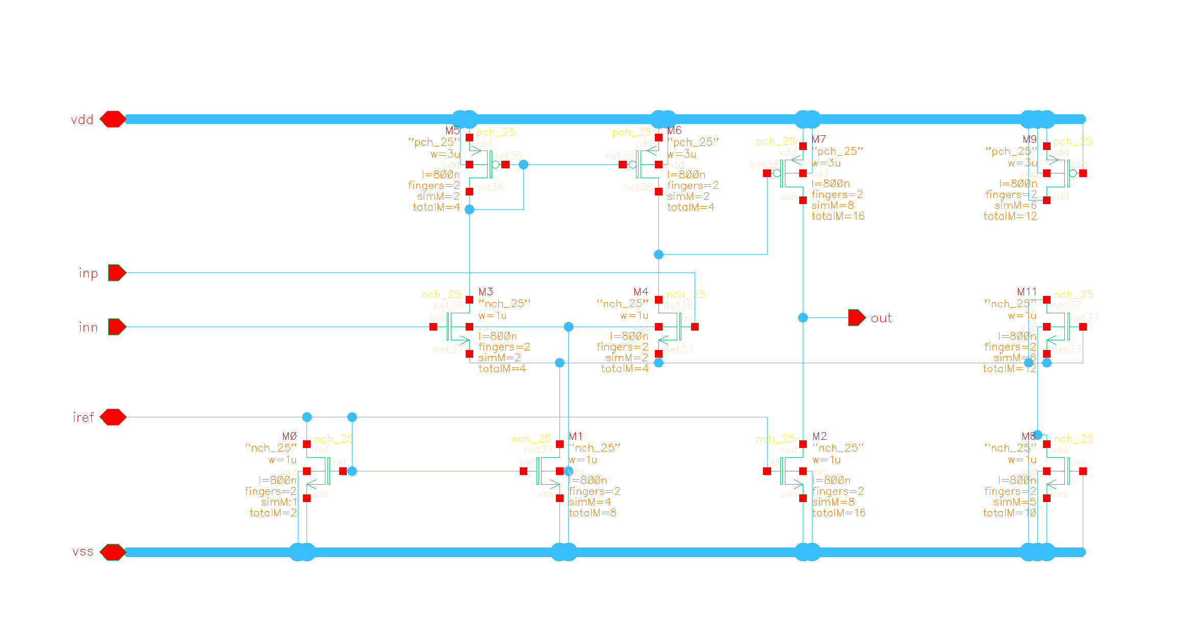
Figure 6. NMOS OTA Comparator
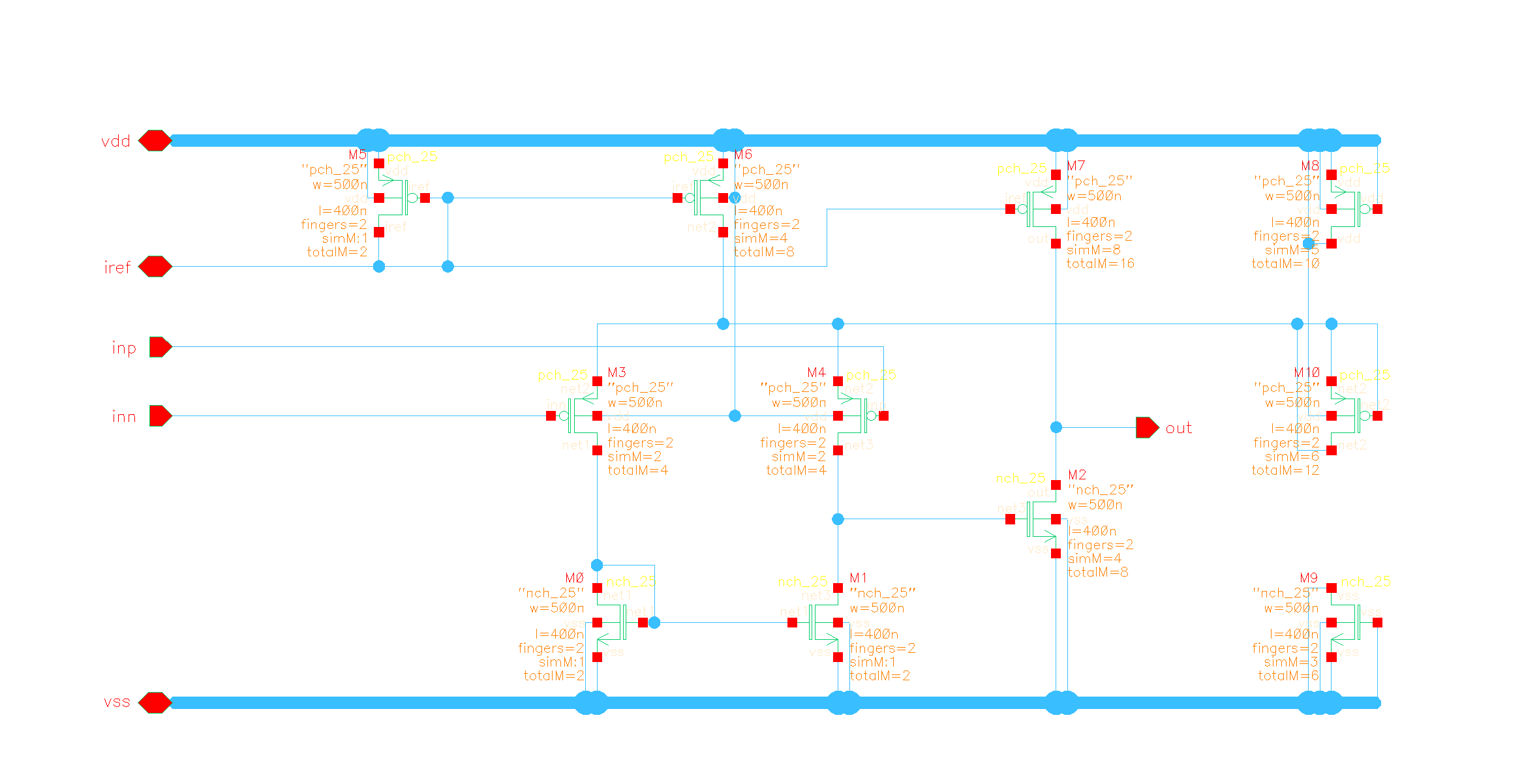
Figure 7. PMOS OTA Comparator
A NMOS differential pair and PMOS differential pair were both chosen to be used for the two comparators. The NMOS differential pair would be used to compare the reference voltage V_High and the PMOS differential pair would be used to compare the reference voltage V_Low. Each comparator was sized with a 20uA first stage and 40uA second stage. These sizes were chosen to ensure low power consumption and similar response times for each stage to ensure the output voltage of the SR Latch would produce a 50% duty cycle clock to be used for the mixer.
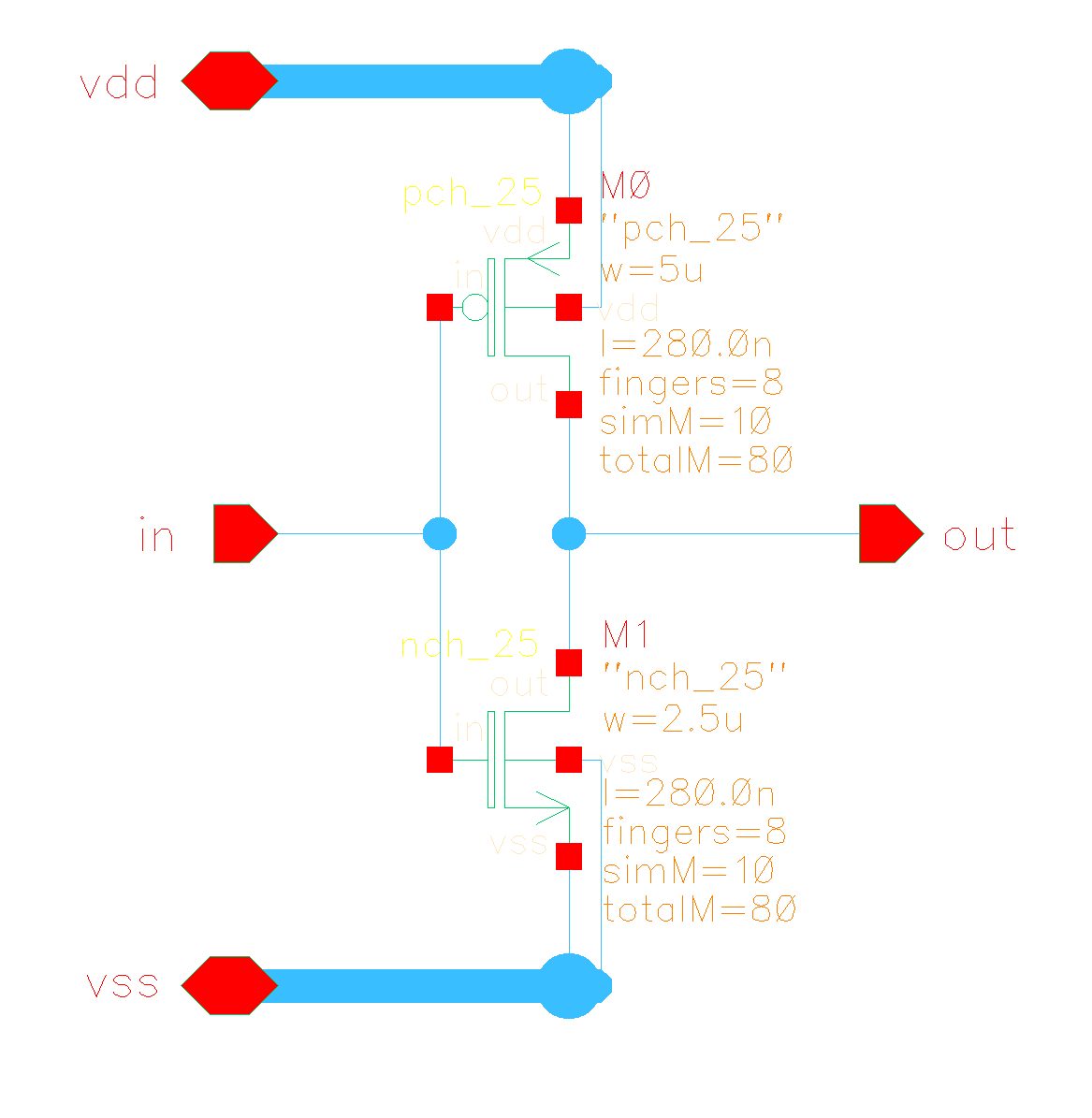
Figure 8. LED Driver Inverter
| R_on | Value (Ohm) |
|---|---|
| Target | |
| NMOS | |
| PMOS |
The final part of the design was developing the variable pulse width voltage to drive the LED. To drive the LED, a simple CMOS inverter was chosen. To provide the 100mA required to drive an LED, the widths and lengths of the PMOS and NMOS of the inverter were sized to provide a low R_on of approximately 10Ohm. To achieve this, the length of the gate was set to the minimum and the width was sized to 400um and 200um for the PMOS and NMOS to achieve the R_on values in the table above.

Figure 9. Hysteresis Comparator for Variable Duty Cycle
To create the variable pulse width, a hysteresis comparator with an NMOS differential pair was used to compare the voltage on the triangle wave to an external voltage reference, V_pw. A hysteresis comparator was chosen over the comparators used for controlling charging to avoid any false triggers from noise. The duty cycle of the voltage reference was designed such that a linear increase resulted in a linear increase in duty cycle. To size the hysteresis comparator, the sizes used for the output comparator from the Analog Front-End were used as this provided >100mV hysteresis. However, to ensure that the comparator could drive the LED driver inverter, the comparator's widths were doubled, which reduced the hysteresis to +/- 89mV.
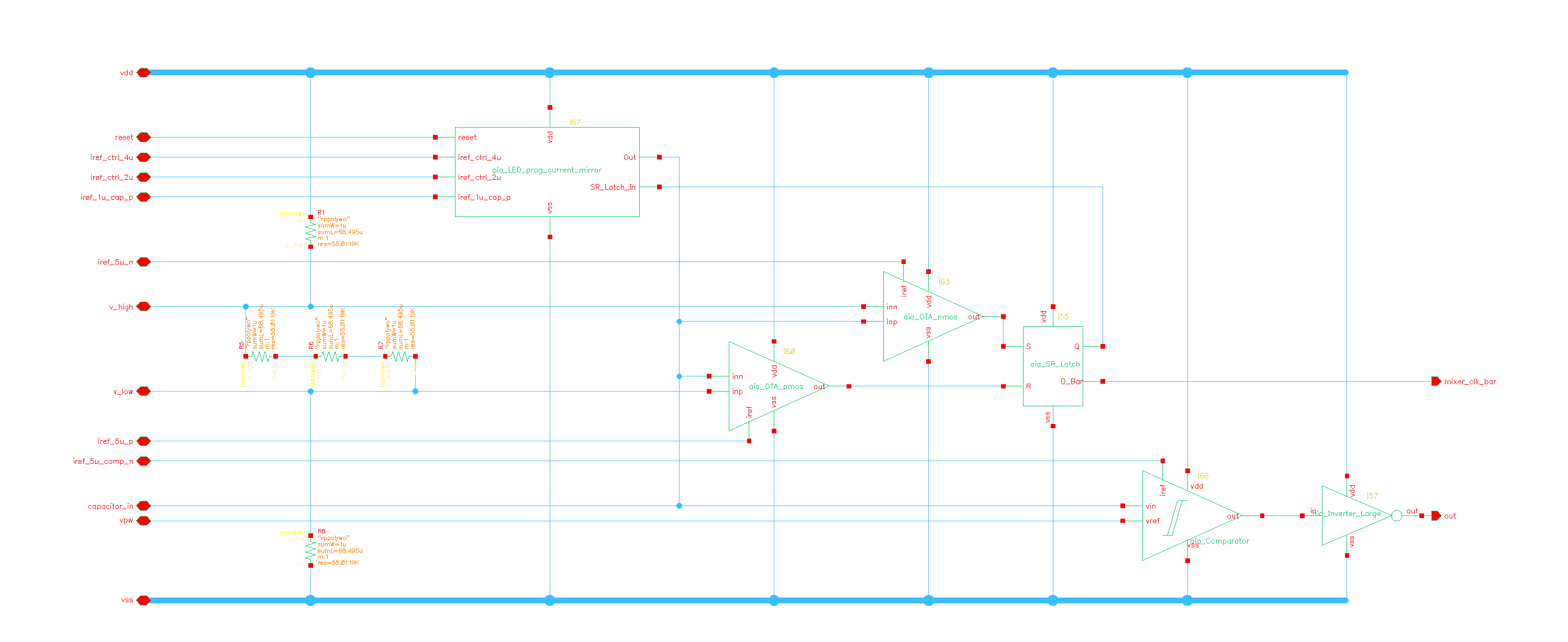
Figure 10. LED Driver Full Schematic
After assembling the blocks, power simulations were run on the LED Driver with a LED modeled by 200Ohm resistor in parallel to a 4pF capacitor. The simulations showed that the LED Driver could provide 30mW to the LED. Due to the high power being transmitted to the LED and wire bond packaging being used for the chip, it was decided to dedicate three pins for the voltage output to the LED, and four pins each for VDD and ground to prevent the high current from burning the wires.
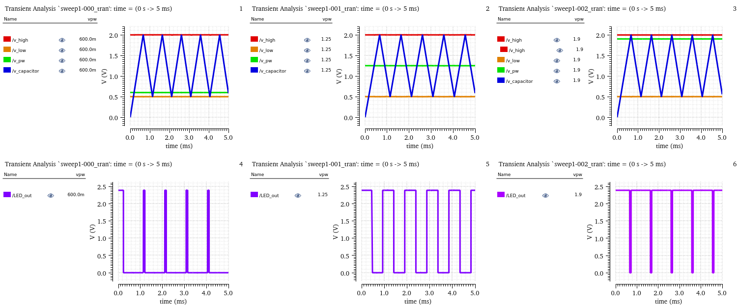
Figure 11. LED Driver Signals (From Left to Right, V_pw = 0.6V, 1.25V, 1.9V)
The graph above shows the LED Driver signal with varying V_pw shown in green. The capacitor's voltage is a triangle wave that is bounded by V_Low and V_High, shown in orange and red respectively. As V_pw increases from 0.6V to 1.9V, the duty cycle on the output voltage to the LED, shown in purple, increases.
Transimpedance Amplifier (TIA)
The design of the Analog Front-End (AFE) began with choosing an appropriate amplifier for the input signal. The PPG signal is transmitted from a photodiode as a current, so to convert this signal into a voltage, a transimpedance amplifier was chosen. Since this was the first block in the AFE chain, the gain of the amplifier was chosen to be as high as possible to minimize the input-referred noise of the AFE. A Miller Operational Transconductance Amplifier (OTA) with a NMOS differential pair with a feedback resistor Rf was chosen for the amplifier design as it provided a high open-loop gain for high linearity with a lower power consumption compared to a PMOS differential pair.
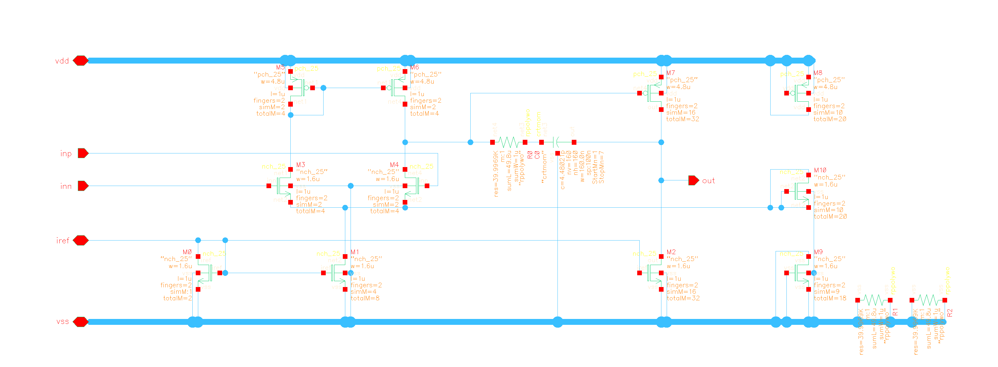
Figure 12. Transimpedance Amplifier OTA Schematic
The design requirements specified to the TIA was a static DC power consumption of 200uA, a target gain of 100kOhm, and needing to drive the low impedance input of the filter. Given the power budget, the power was split 40uA to the first stage and 160uA to the second stage to be able to drive the filter's input impedance, while ensuring the noise on the first stage would be small. A gm/Id of 10 was used as a metric to help determine the size of each transistor.
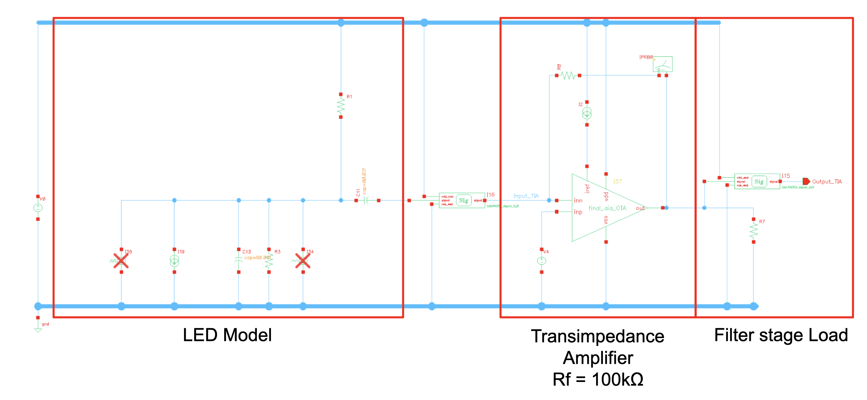
Figure 13. Transimpedance Amplifier Testbench
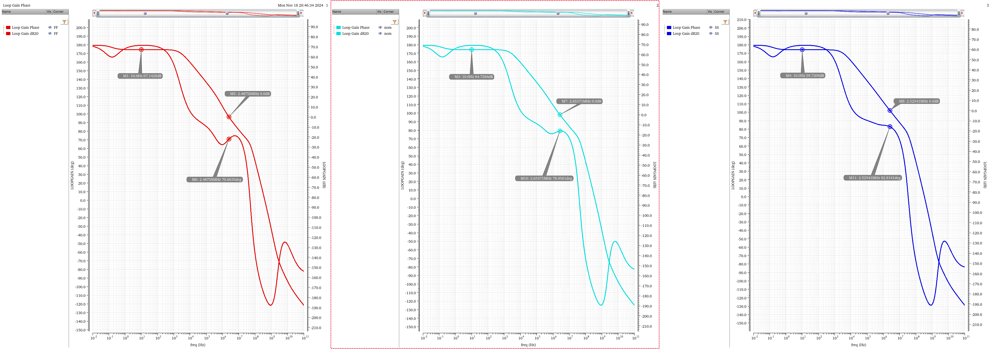
Figure 14. Loop Gain and Phase of Transimpedance Amplifier
To ensure accurate modeling of the TIA's stability, the load of the filter and the biasing network of the photodiode were taken into account. Initial simulations showed that the low input impedance of the filter reduced the loop gain from 80dB to 60dB. A minimum phase margin of 60deg in the FF corner was chosen to ensure small overshoot and a fast response from the TIA across PVT. To achieve this phase margin, a pole-zero compensation network was used as the TIA's high loop gain required pole-zero compensation. A zero at approximately 900kHz was chosen as calculations showed it would produce approximately 60deg based on the poles in the FF corner. This resulted in a pole-zero compensation network with a capacitor of 4.48pF and a resistor of 40kOhm, and a phase margin of 66deg in the FF corner.
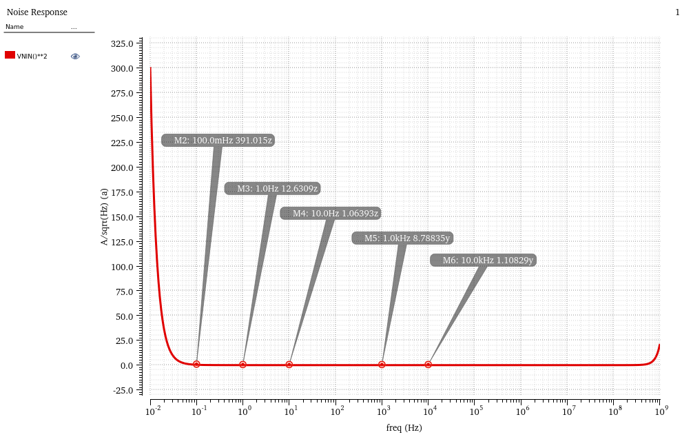
Figure 15. Noise Simulation of Transimpedance Amplifier
As the TIA is the first block in the analog front-end, noise analysis of the TIA was critical to minimize the input referred noise of the system. Since the PPG signal from lab measurements of the photodiode was determined to be 10nA and a SNR of 10 was required, the TIA needed to have an input referred noise of less than 1nA. From simulations around the frequency range of the system, it was found that the noise from the TIA was approximately 0.74nA with the dominant noise source being flicker noise of the first stage. In addition, the feedback resistor Rf was moved off-chip in the event more gain from the TIA was needed to reduce the system's noise.
Mixer
![Mixer Schematic [2]](./images/Schematic_Design/Mixer_literature_source.png)
Figure 16. Mixer Schematic [2]
To achieve the desired high-frequency signal demodulation and noise shaping behaviors of the HF chain, a search for a mixer topology which would allow the chip to access these effects with minimal need for additional control signals since at this point in the design process, almost all of the I/O pins had been budgeted, so each additional signal would necessitate the removal of a control signal / testpoint from another block. To do this, a topology from [2] was modified into the below topology:
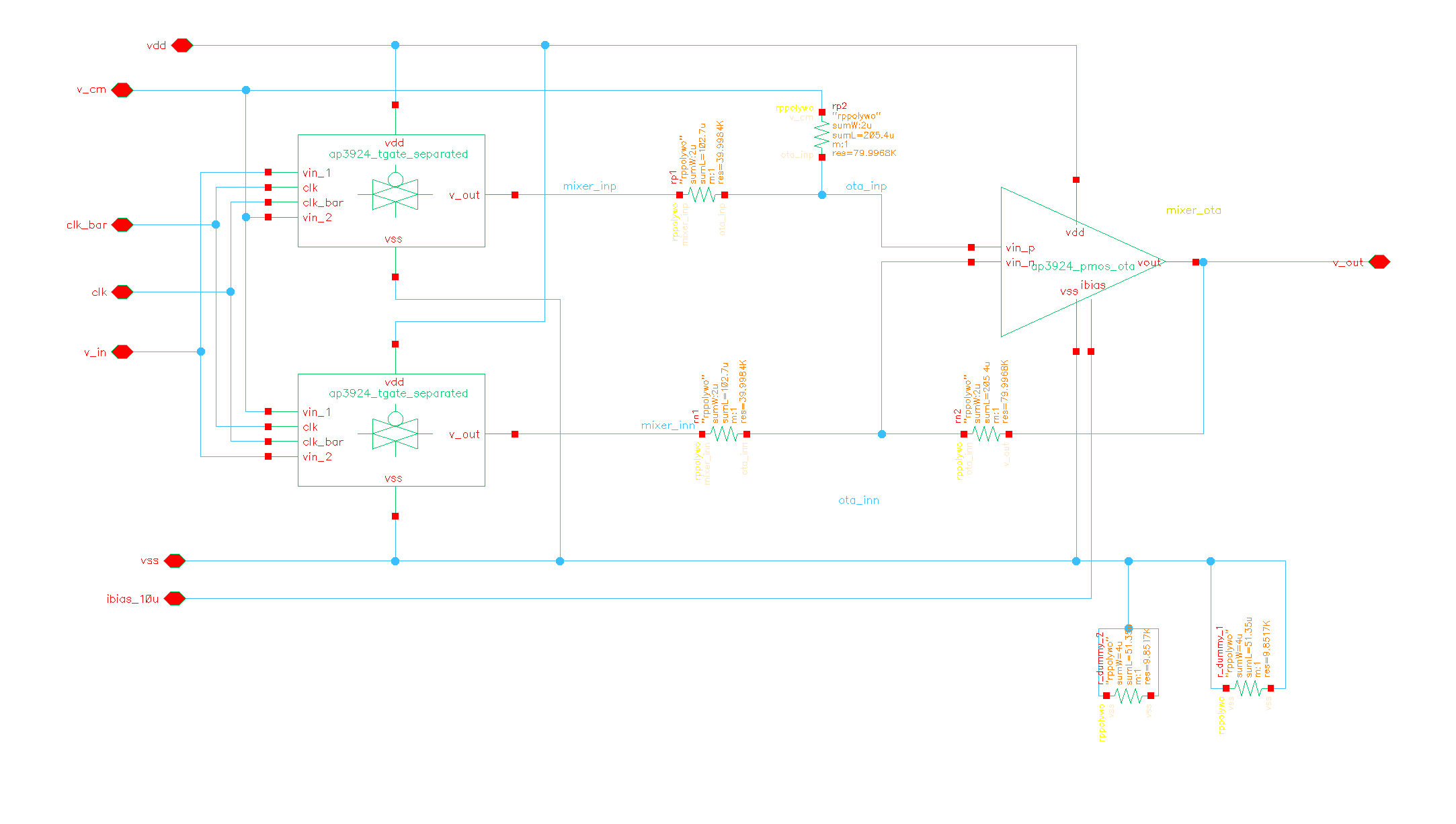
Figure 17. Top-level Mixer Schematic
This circuit above met all of the desired requirements for the chip's mixing needs. The +1/-1 amplification style would allow demodulation through linear components and signals already being produced on-chip (i.e., a 50/50 clock from the LED driver). To remove the need for a tuning voltage, the transmission gate was designed to have relatively low impedance which was placed in series with polysilicon resistors - this linearized the gain expression to be:
Phi: Av = (+)(rp2/(rp1+rp2))*((rn1+rn2)/rn1) = +rn2/rp1 with rn1=rp1=r1, rn2=rp2=r2
Phi_bar: Av = (-)rn2/rn1

Figure 18. Loop Gain and Phase of Mixer OTA
The OTA used for gain in this circuit was designed to have a loop-gain of 50dB, a high bandwidth of 10.9MHz, and a phase margin of 90.2deg to maintain a high closed-loop accuracy and fast settling time, given the frequent and precise +1/-1 switching behavior it needed to maintain.
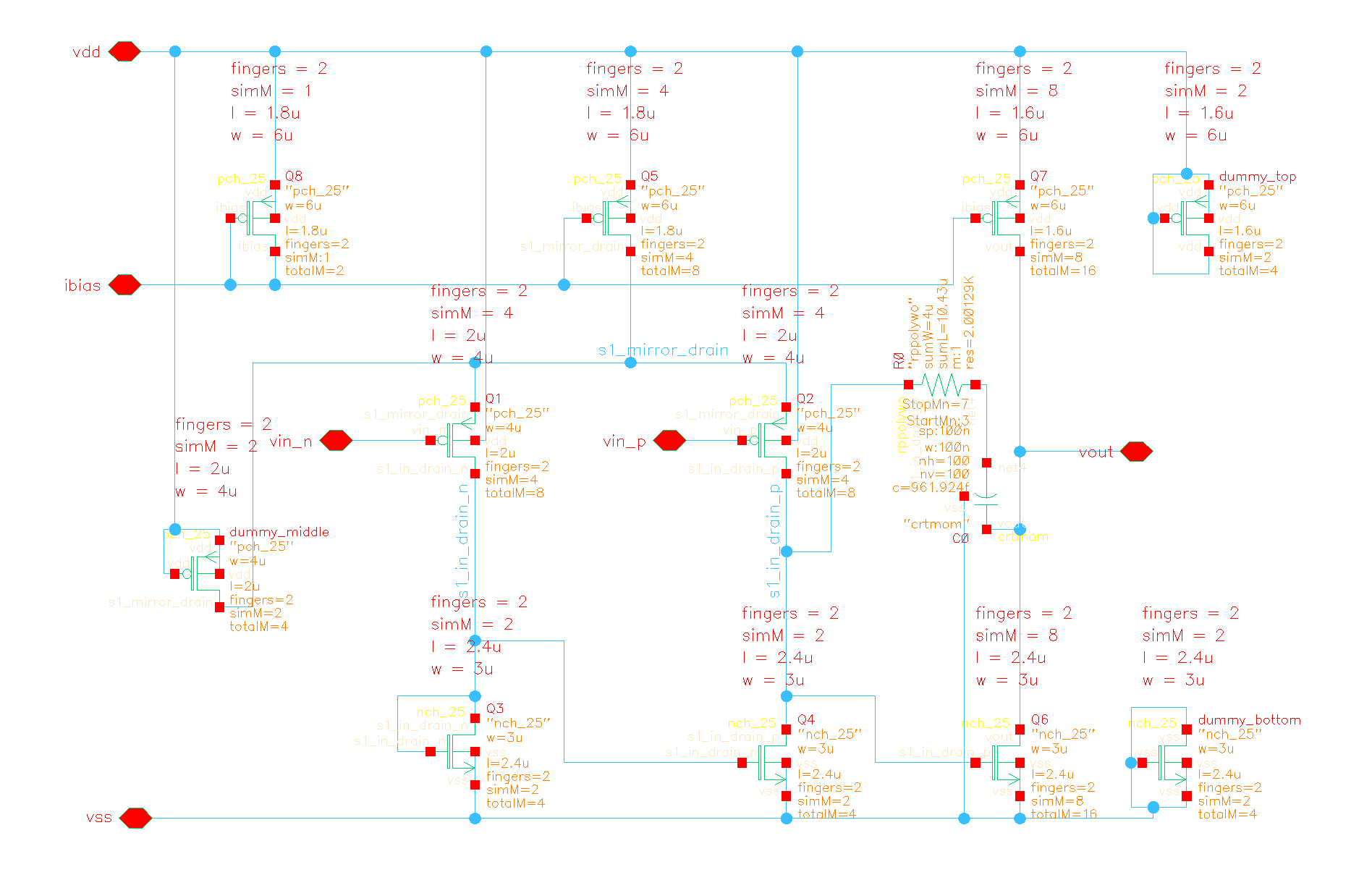
Figure 19. Mixer OTA Schematic
The transmission gate was built from two sets of complementary pass transistors, fed opposite complementary clock signals, with each pair having an effective parallel r_on of 50Ohm. This r_on value is excessively low (~1% of the linear resistor values) and could have tolerated higher parasitics on these paths. However, due to a lack of strict area constraints on the floorplan, issues with charge injection being not observed, these blocks were kept as initially designed. The clock used for the Mixer is produced by the LED Driver and is propagated to the mixer block via an inverter chain, before being split into clk and clk_bar directly before use.
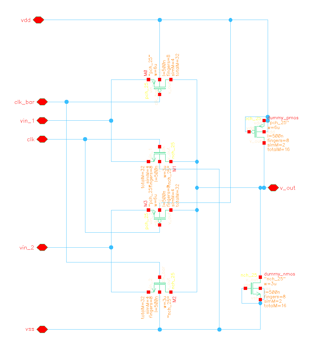
Figure 20. Mixer Transmission Gate Schematic
Mossberg-Ackerberg Filter
In designing a filtering stage between the preamplifier and programmable gain amplifiers, the goal was to obtain moderate, steady gain within the passband (0.8-2.4Hz) while rapidly attenuating above and below this range - in the PPG use case, motion artifacts often appear as step functions in the time domain, so the filtering stage needed a fast attenuation of DC and low-frequency terms. Thus, it was decided to use a cascade of two bandpass biquads, allowing 40dB/decade attenuation outside of an even passband, realized by staggering the two BPFs around the desired narrowband range (0.8-2Hz).

Figure 21. Mossberg-Ackerberg Filter Schematic
The advantage of this topology over a Tow-Thomas biquad lies in the cancellation of losses from phase non-idealities in the non-inverting integrator. Furthermore, as with a Tow-Thomas topology, all gain/Q terms could be realized by ratios of like components on-chip, and the corner frequencies could be set with off-chip capacitances after tapeout.
Figure 22. Filter OTA Schematic
The primary drawback of this topology lies in its power consumption, as each biquad uses 3 OTAs. However, given the target power budget of the chip, the filter was able to keep within its allocated power budget, even with two cascaded stages, so the filter block was kept to this scale.
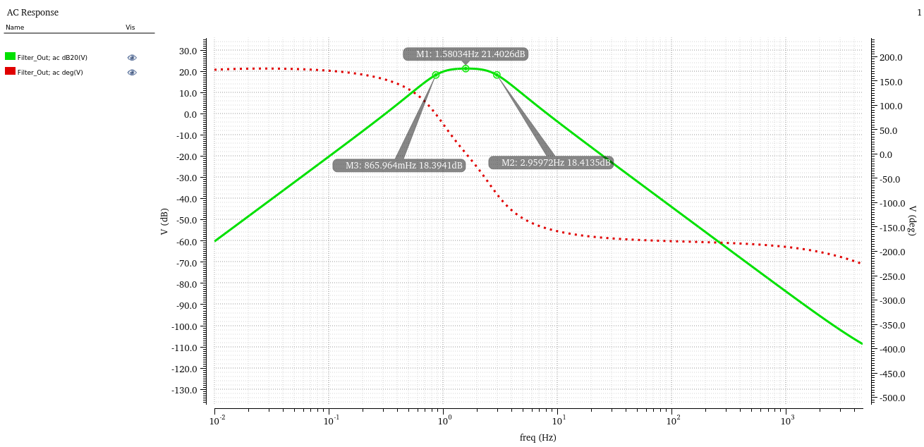
Figure 23. Filter AC Response
Programable Gain Amplifier
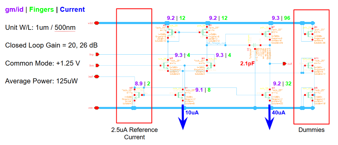
Figure 24. Programmable Gain Amplifier OTA Schematic
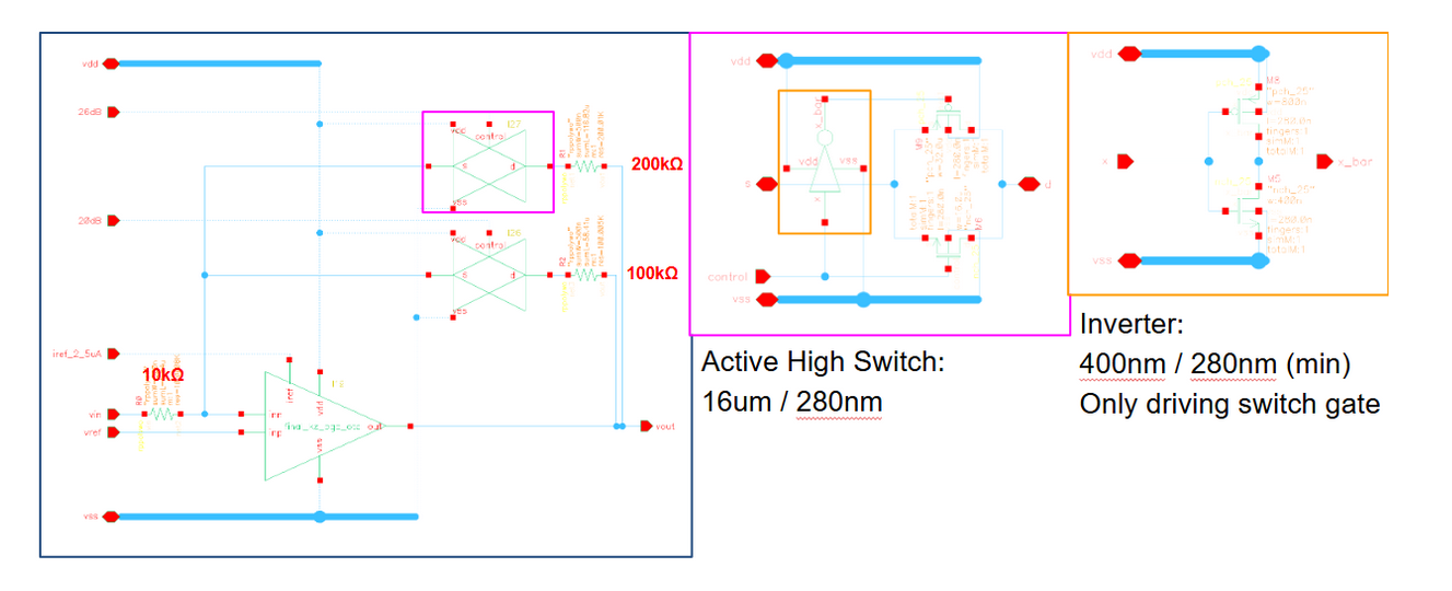
Figure 25. PGA, Active High Switch, and Inverter Schematics
To amplify the PPG signal into a large voltage for 1-bit A/D conversion, programmable gain amplifiers, PGAs, were added to the signal chain. The PGA was implemented as two identical stages, each with a two stage operational transconductance amplifier placed in an inverting topology. Two feedback resistors are digitally controlled using low R_on switches, allowing for ~16.5dB, 20dB, or 26dB of gain. This implementation minimizes power consumption while being flexible with gain variability.
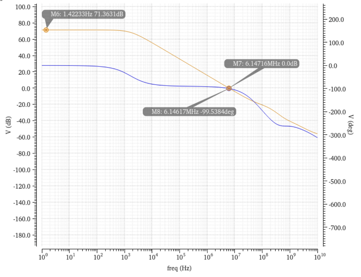
Figure 26. PGA Loop Gain and Phase
The PGA featured Miller compensation, using only a capacitor, to ensure stability over pole-zero compensation since PGA did not need a large bandwidth. Using this compensation technique, the first pole of the PGA was placed at 720Hz. Overall, the PGA achieved a loop gain of 71.4dB and a phase margin of 80deg.
Comparator
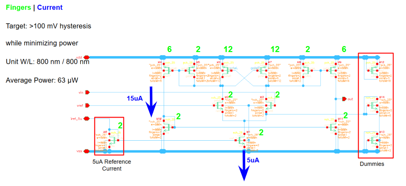
Figure 27. Comparator Schematic
After the PPG signal was amplified by the PGA, the comparator was used for 1-bit A/D conversion to an Arduino to extract the heart rate signal. The comparator was implemented using the topology above. It was designed for >100mV hysteresis to tolerate 1/f noise amplified along the signal chain and prevent the digital output from incorrectly switching. The magnitude of hysteresis is controlled by the size of M7 and M2 relative to M5 and equivalently, the size of M6 and M3 relative to M8, which are equal for symmetric hysteresis.
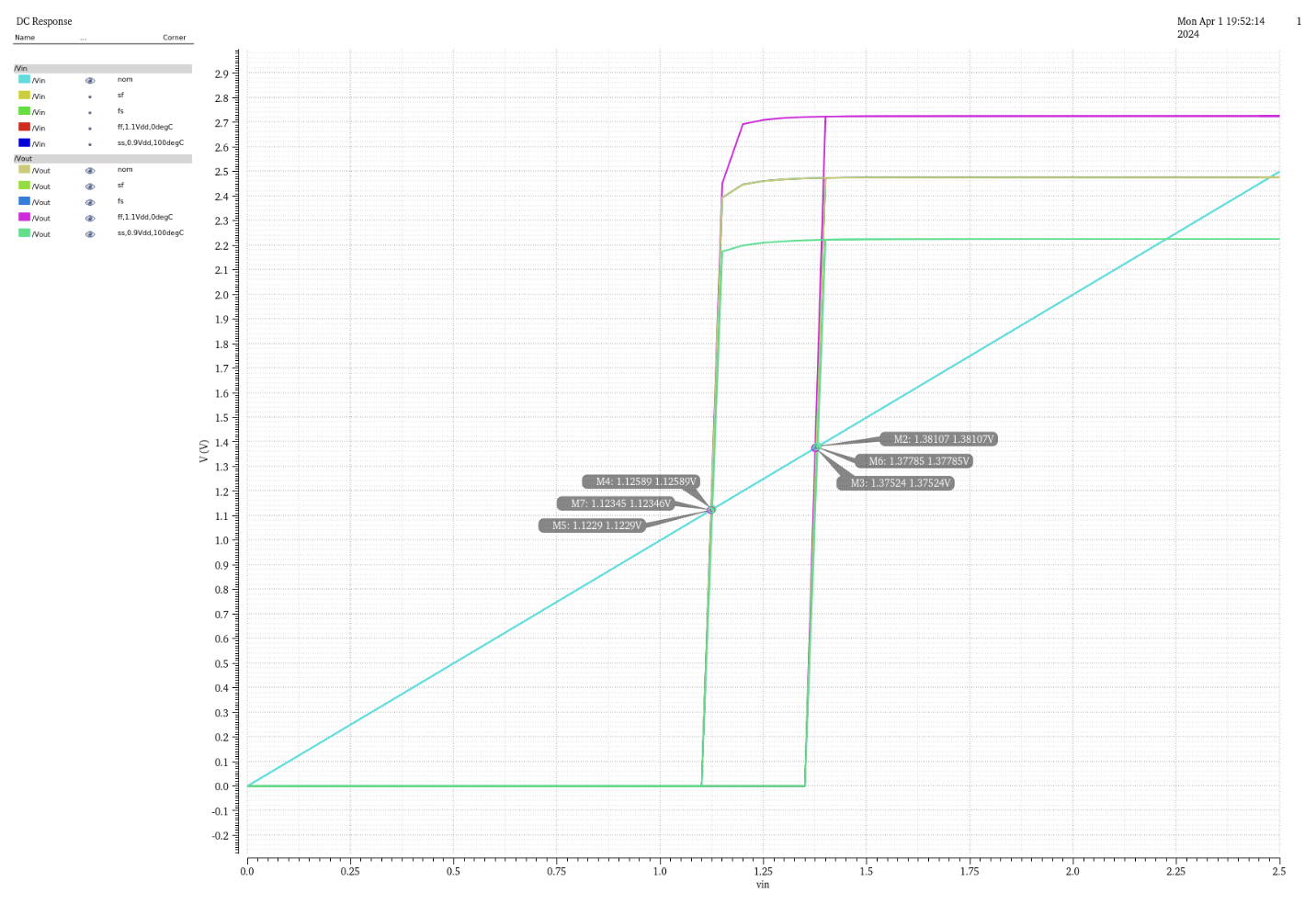
Figure 28. Comparator's DC Response
As shown in the figure above is the DC Response of the comparator for 1.25V reference across PVT. The actual hysteresis of the comparator is +/-127mV. With positive feedback, the comparator is able to drive a sharp square wave while consuming the least power in the signal chain.
Master Current Mirror (MCM)
Figure 29. Master Current Mirror Schematic
Due to pin limitations and many current references needed on chip, a master current mirror was created. The purpose of this block was to group together the reference current for a group of blocks. The grouping was chosen to give each designer a current reference. This resulted in four current references, a 5uA reference for the LED Driver, a 10uA for the TIA, a 10uA reference for the Filter and Mixer, and a 2.5uA reference for the PGAs and Comparator. The sizing of the MCM was determined by trying to minimize the effect of channel length modulation and ensure a small error in the mirroring current's value from the reference current.