
PCB Design
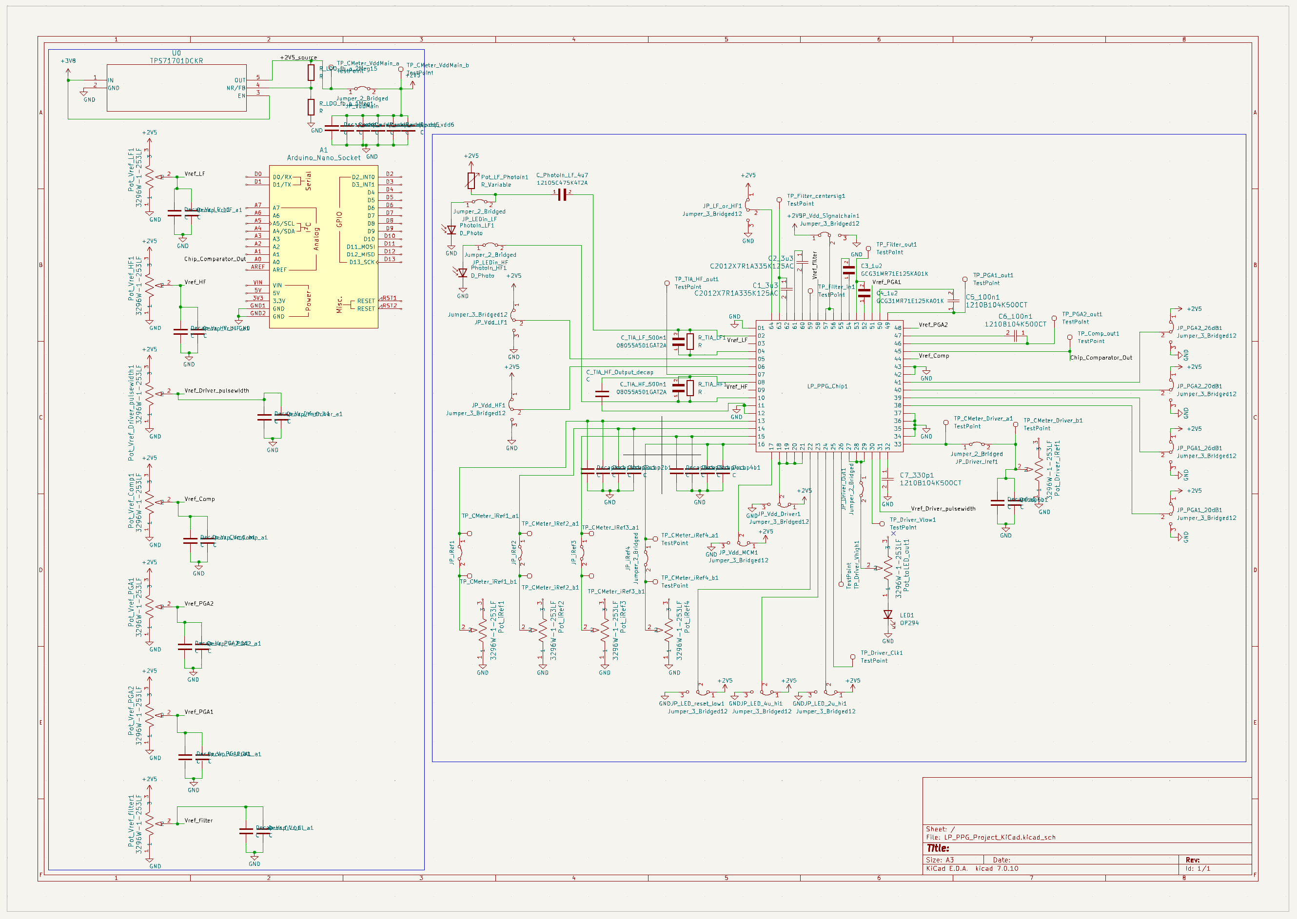
Figure 1.PCB Schematic
In performing post-silicon validation of the chip, a PCB was developed that would allow independent evaluation of performance and power consumption of each block within each signal chain on the chip. PCB design was completed using the KiCAD PCB design suite, with footprints and models taken from Mouser, from which the parts were obtained.
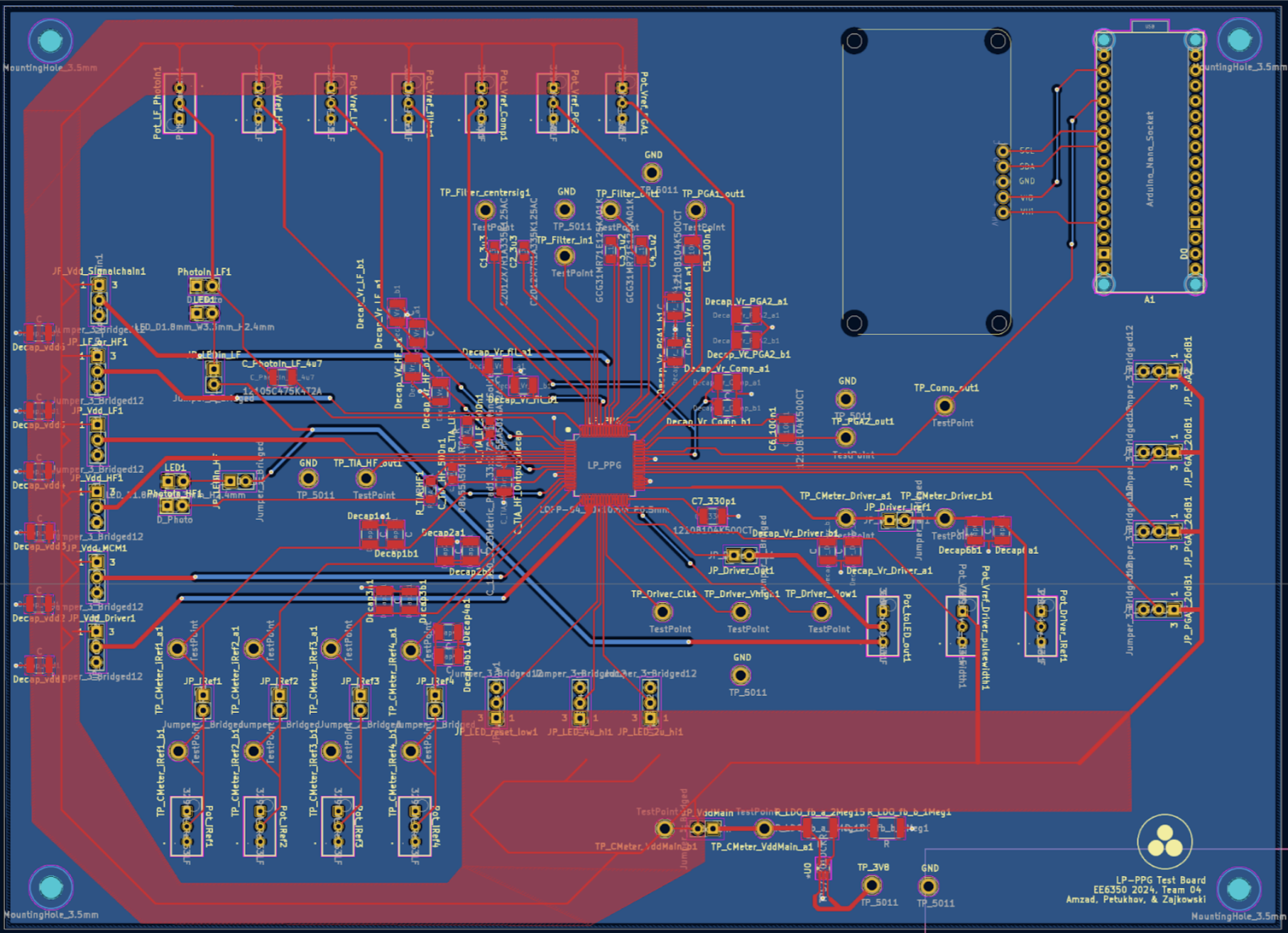
Figure 2. PCB Layout
Physical layout of the PCB was straightforward following the floorplanning completed in the physical design in the Spring. The chip operated on five power domains, each individually toggled via the array of jumpers on the left side of the board. The main 2.5V VDD rail is produced at the bottom of the board via a Low Drop-Out (LDO) regulator with 2.8-7V input range. Empty space was left aside the LDO subcircuit to attach a 3.7V lithium-ion cell, although in testing and demonstration, the device was powered from a 3V DC power supply.
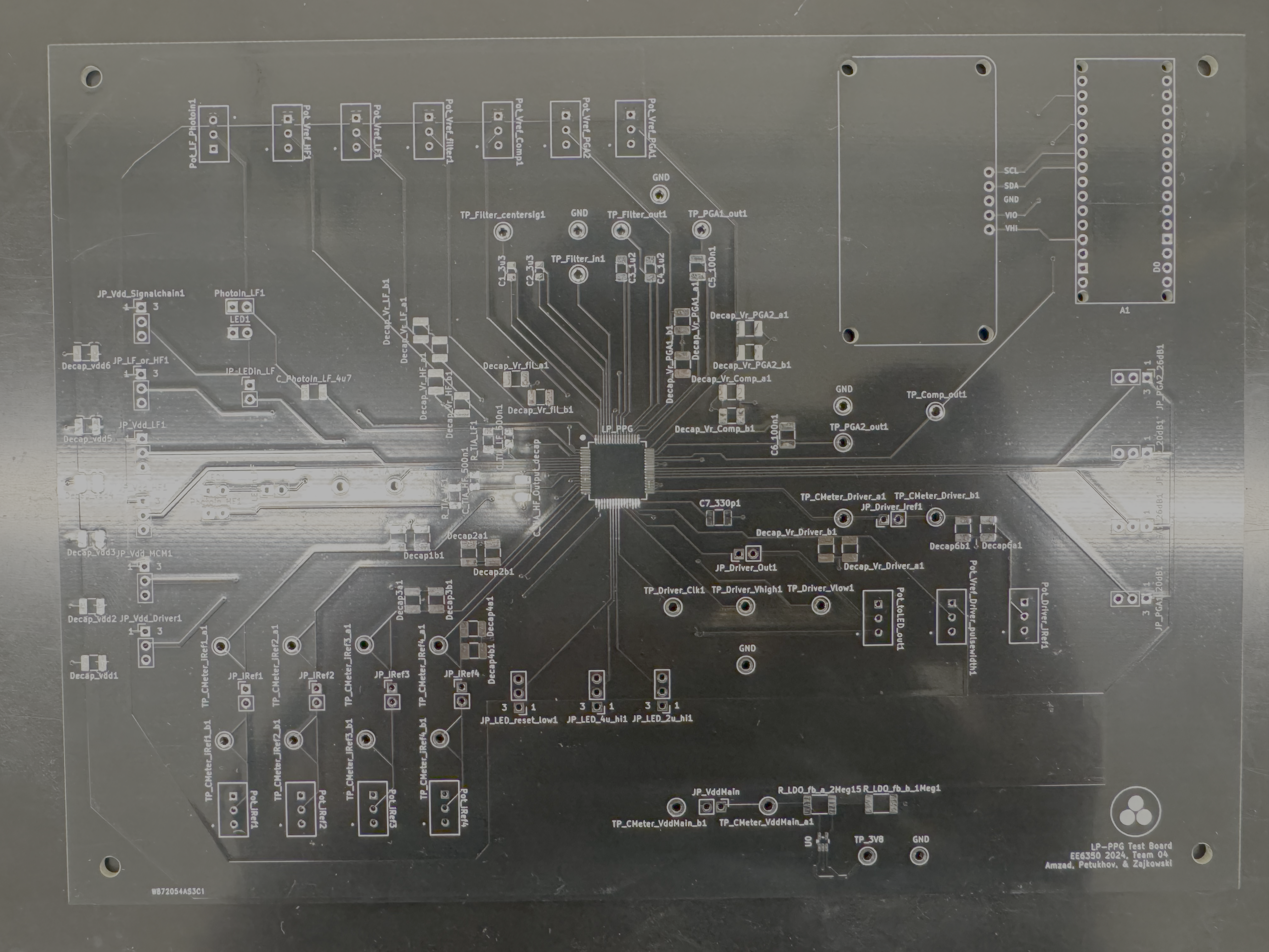
Figure 3. Fabricated PCB
During actual testing, initial static power characterizations were performed by disconnecting unused power domains from their respective VDDs and bias currents. Since the OTAs used in all parts of the signal chains consume constant currents regardless of current being diverted to their loads, dynamic power consumption for the majority of systems on the chip was not required. For the LED driver, dynamic power consumption was calculated using a multimeter current probe to express the time-averaged current pulled by the block across duty cycles, even though given the relatively small overhead of the driver circuitry, the power consumption vs duty-cycle could be predicted quite linearly down from 100% drive strength.
In behavioral testing, every key node on the signal chain was given a testpoint. Beyond these testpoints, additional nodes could be accessed via pads on the passive components. Careful consideration was given to include redundant ground testpoints around all areas where oscilloscope probes were intended to be attached during testing and demonstration. Additional space in the top right corner was provided to allow an Arduino Nano and alphanumeric display modules to be soldered into place on the testboard with relevant power & signal connections made on-board.