
Physical Design
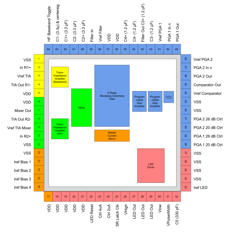
Figure 1. Floorplan and Pinout of Chip
The floorplan of the chip was created with the goal of distancing the Analog Front-End from the noise of the LED Driver Inverter. To achieve this, the bottom of the chip was allocated to the LED Driver and the top was allocated to the Analog Front-End. The chip was split into five power domains, represented in the figure above by the five different colors, to be able to turn off certain power domains during testing. The floorplan also tried to optimize the use of symmetry of blocks to help produce better matching. For this reason, the two TIAs were mirrored to one another, the filter had a line of symmetry down the middle, and the two PGAs were placed close to each other.
For the global routing of the chip, Metal 8 and Metal 9 were allocated for routing to the ESD pads. Due to the low frequency range of the system, the impedance of each line was dominated by the resistance, which led to the use of wide metal traces in order to reduce the resistance of the lines when routing. Additionally, the lines were spaced out by 10µm to minimize any crosstalk that could occur. In terms of the power grid, star grounding was used to help mitigate voltage drop from high current circuits such as the driver inverter in the LED Driver.
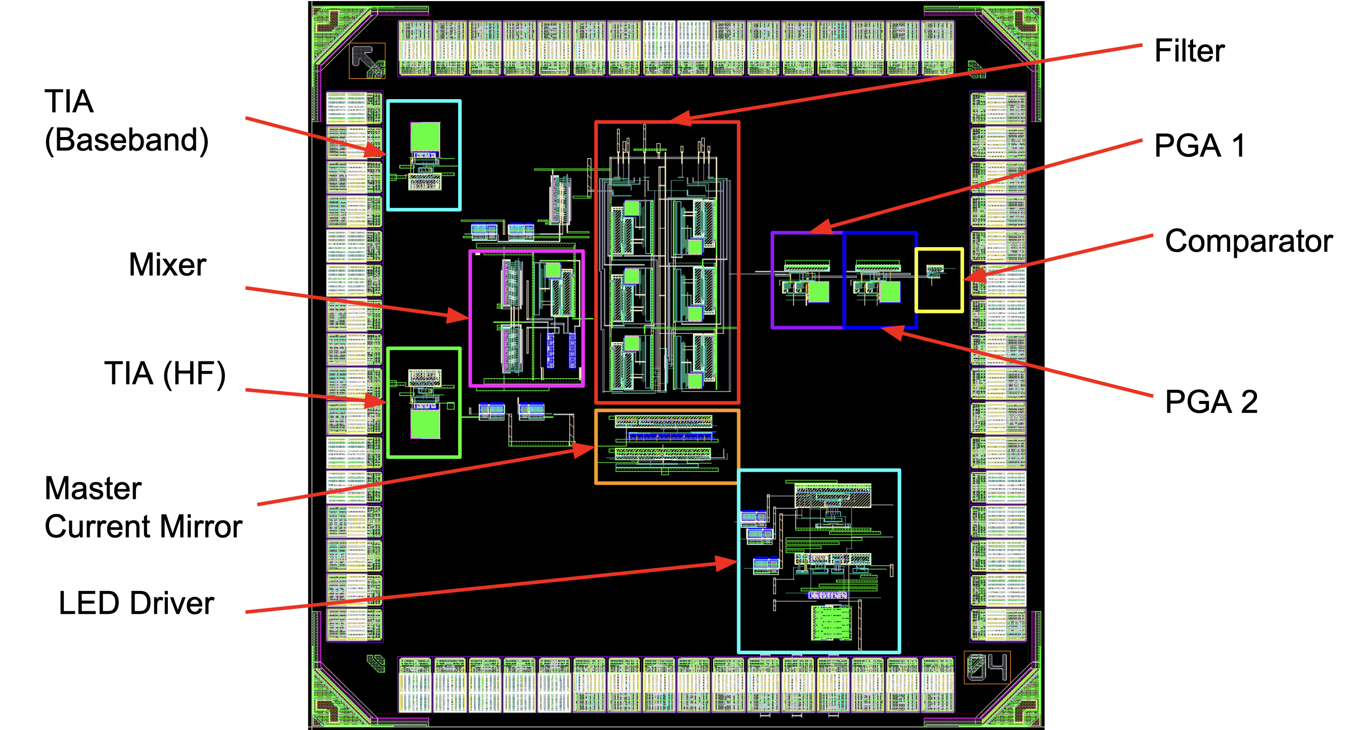
Figure 2. Layout Showing Locations of Blocks
After global routing was complete, each digital pin was given a schmitt buffer to ensure that the external reference would be able to drive the digital circuit. Since the bond wire package had such a high inductance value, it was found that the filter's frequency response would flatten out at high frequencies. For this reason, small MOM-capacitors were added on chip between the filter's capacitor nodes to help filter higher frequencies. In addition, on-chip decoupling capacitors, decap, using NMOS devices were added in empty areas of the chip to reduce power supply noise. A majority of the on-chip decap was given to the LED Driver due to its large current draw.
In terms of the physical design of individual circuits, symmetry was prioritized to provide good matching between transistors while minimizing gradients. Dummy devices were inserted to minimize the effect of Shallow Trench Isolation. The N-well region of the PMOS devices were increased to minimize the Well Proximity Effect. Guard rings around PMOS and NMOS devices were also inserted to prevent any potential latch-up issues. Additional dummy resistors were also placed around critical resistors to provide better matching. Multiple vias were also used between metal layers for additional reliability and lower resistance.
Below are images of the layouts of the full chip and individual blocks.
Full Chip
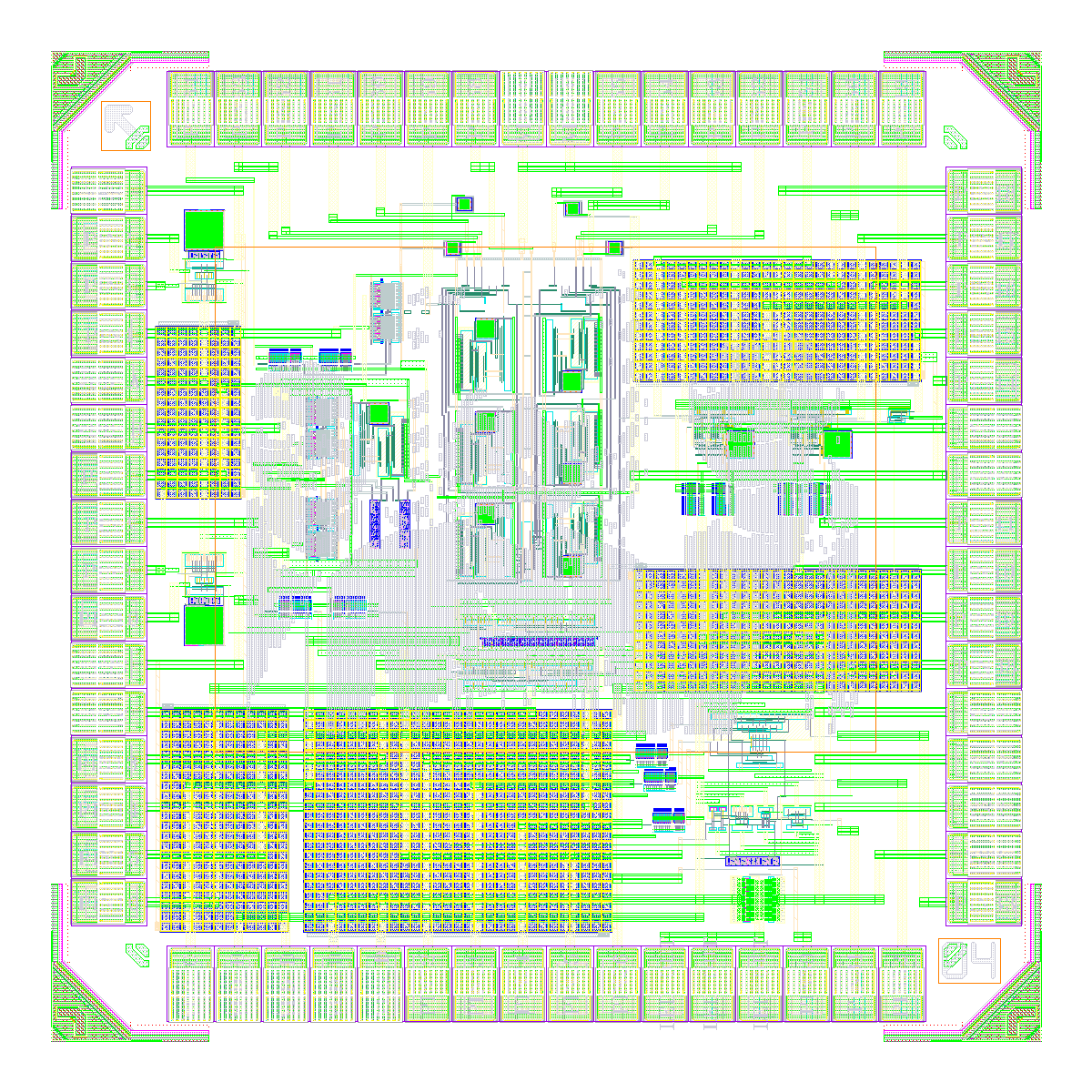
Figure 3. Full Chip Layout
LED Driver
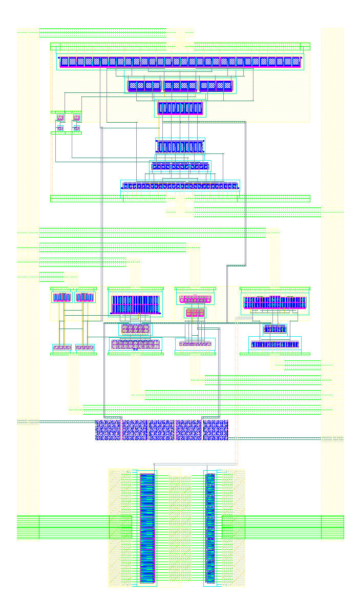
Figure 4. LED Driver Layout
Transimpedance Amplifier
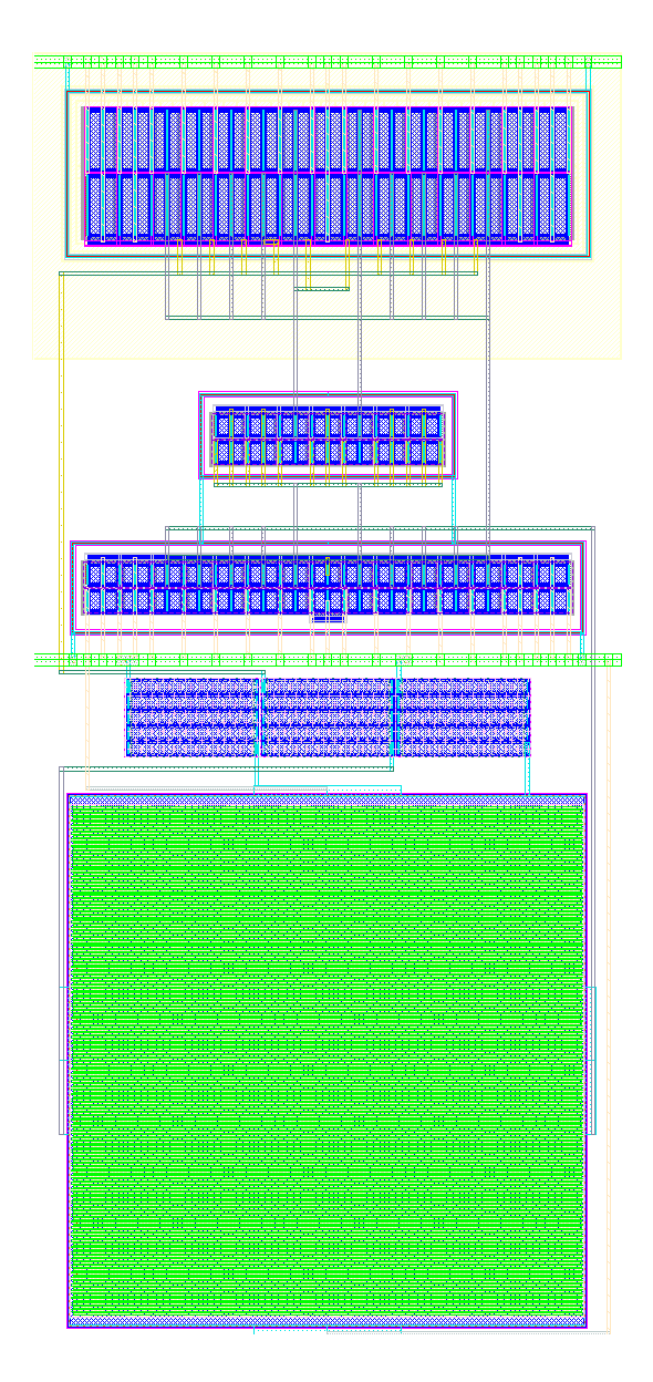
Figure 5. Transimpedance Amplifier Layout
Mixer
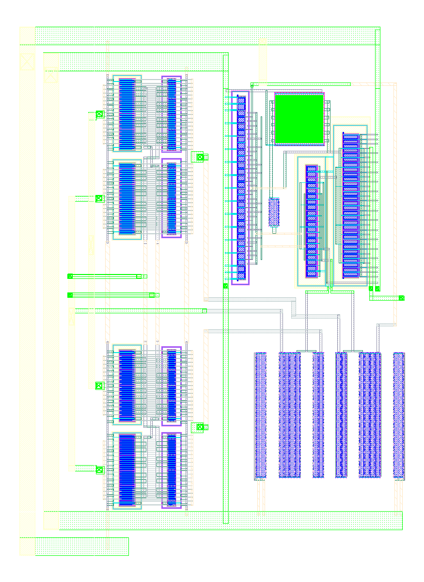
Figure 6. Mixer Layout
Mossberg-Ackerberg Filter
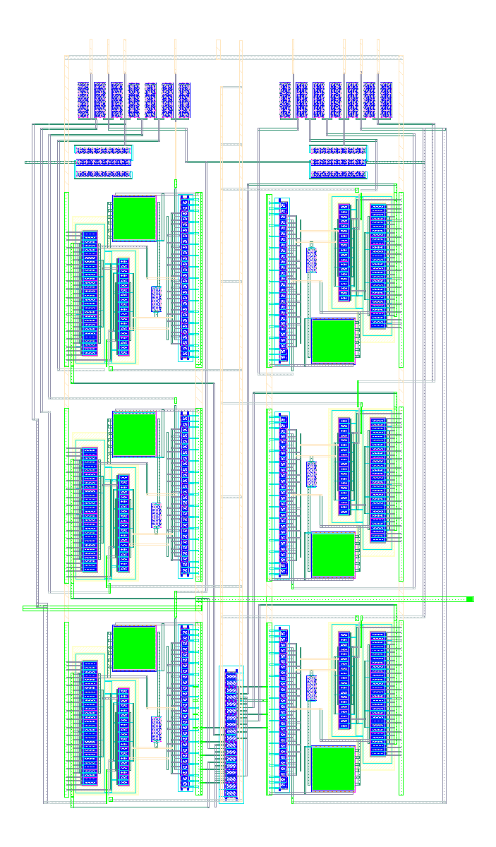
Figure 7. Mossberg-Ackerberg Filter Layout
Programmable Gain Amplifier
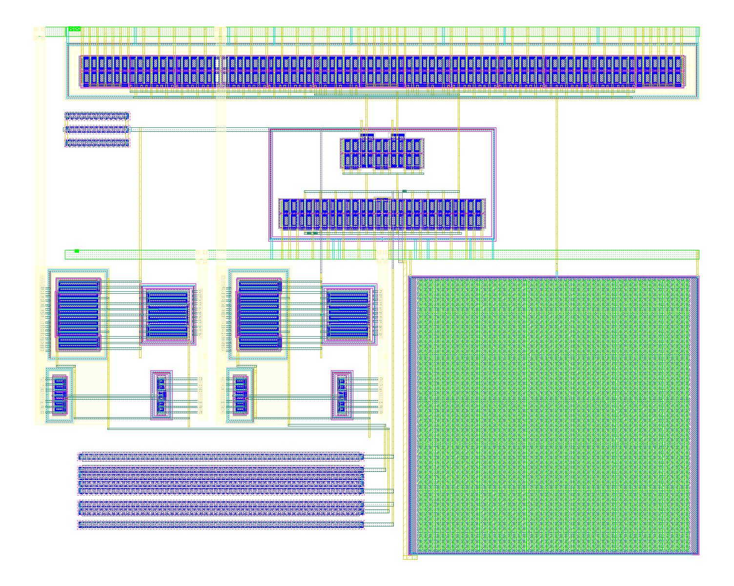
Figure 8. Programmable Gain Amplifier Layout
Comparator
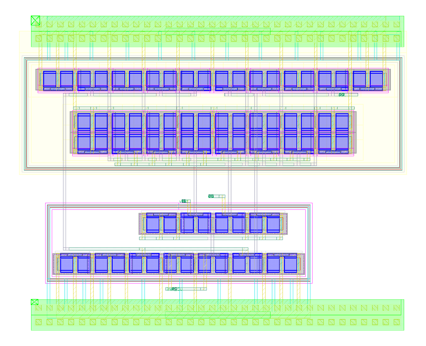
Figure 9. Comparator Layout
Master Current Mirror
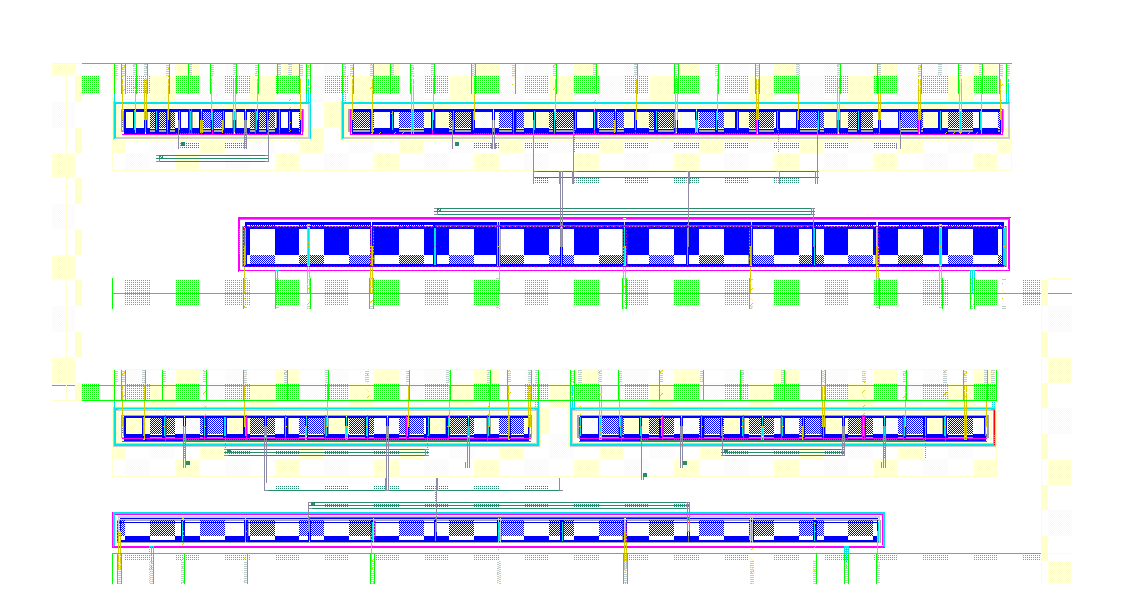
Figure 10. Master Current Mirror Layout